

Method of manufacturing a semiconductor device
a manufacturing method and semiconductor technology, applied in the direction of transistors, optics, instruments, etc., can solve the problems of difficult channel formation regions, inability to precisely control the position of crystal aggregates with conventional techniques, and large size of crystal grains obtained, etc., to achieve the effect of suppressing tft variations
- Summary
- Abstract
- Description
- Claims
- Application Information
AI Technical Summary
Benefits of technology
Problems solved by technology
Method used
Image

Examples
embodiments
Embodiment 1
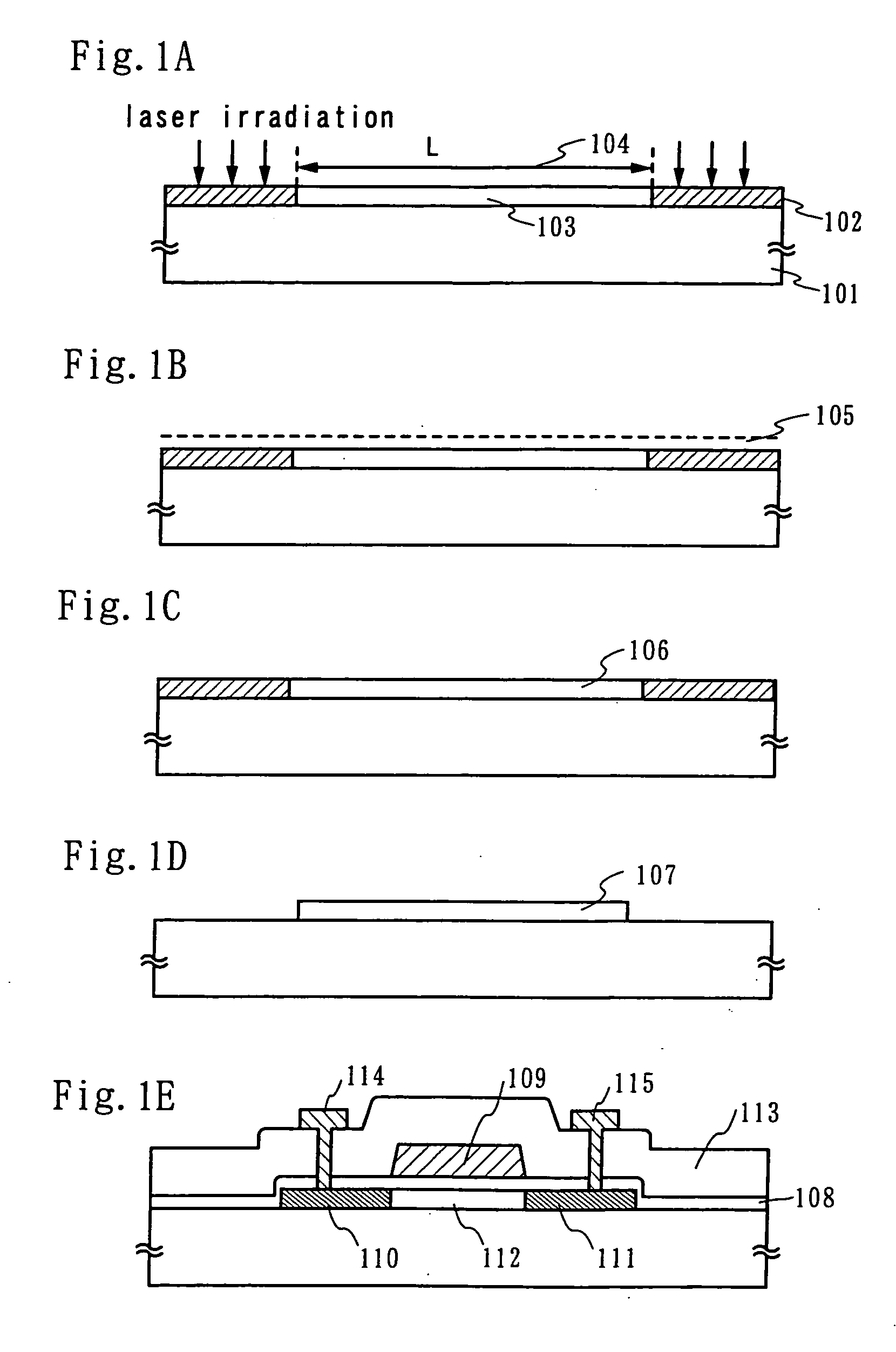
[0053] Embodiment 1 relates to a technique of suppressing TFT variation by forming an amorphous semiconductor film on a quartz substrate, performing selective laser light irradiation to selectively form independent amorphous semiconductor thin films, introducing a metallic film for promoting crystallization to the amorphous semiconductor films, crystallizing the independent amorphous semiconductor thin films by using heat treatment, and as a result, arbitrarily controlling the position of crystal aggregates (domains).
[0054] A process of manufacturing a crystalline semiconductor film of Embodiment 1 is shown in FIGS. 1A to 1E. First, a 50 nm thick amorphous silicon film is formed on the quartz substrate 101 by reduced pressure thermal CVD. Laser light is then selectively irradiated to the amorphous silicon film 102. Further, the amorphous silicon film 103 not yet irradiated is later used for a TFT formation region. If L (reference numeral 104) is taken as the length of...
embodiment 2
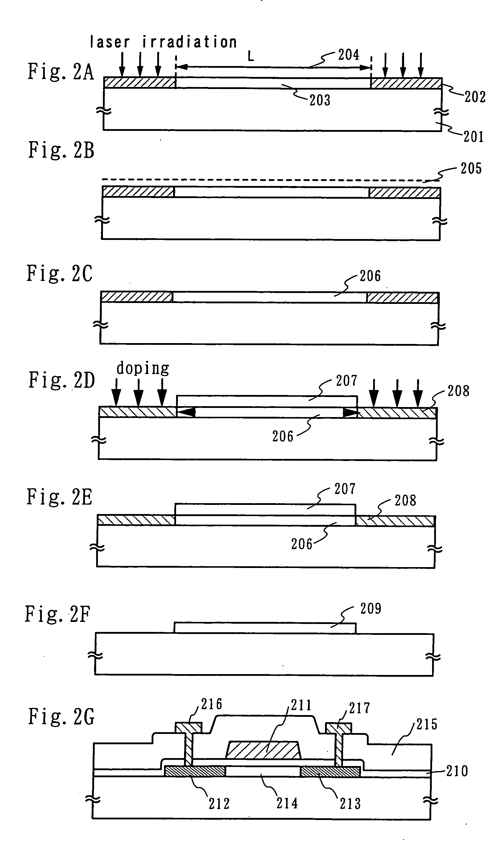
[0065] Embodiment 2 relates to a technique of suppressing TFT variation by introducing a metallic film for promoting crystallization to an amorphous semiconductor film, crystallizing independent amorphous semiconductor thin films by heat treatment, performing gettering processing in order to remove a metallic element from, or reduce the concentration of the metallic element in, the crystallized semiconductor films, and as a result, arbitrarily controlling the location of crystal aggregates (domains).
[0066] A process of manufacturing a crystalline semiconductor film of Embodiment 2 is shown in FIGS. 2A to 2G. First, a 50 nm thick amorphous silicon film is formed on the quartz substrate 201 by reduced pressure thermal CVD. Laser light is then selectively irradiated to the amorphous silicon film 202. Further, the amorphous silicon film 203 not yet irradiated is later used for a TFT formation region. If L (reference numeral 204) is taken as the length of the amorphous silicon, then L≦2...
embodiment 3
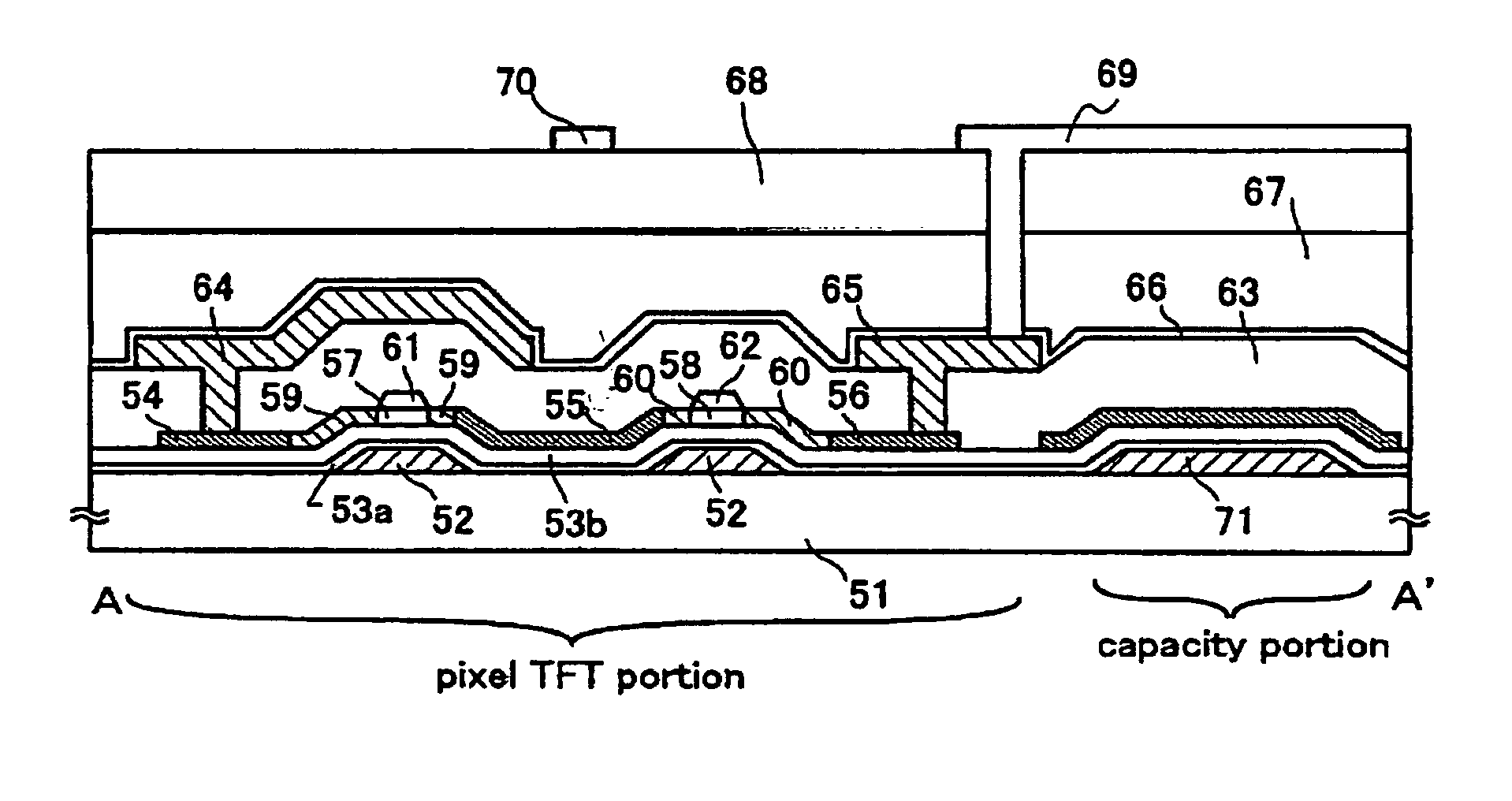
[0079] Described here is a method of manufacturing a liquid crystal display device using an active matrix substrate which has a pixel portion. The description will be given with reference to FIGS. 4A to 8A2.
[0080] An active matrix liquid crystal display device that uses a TFT as a switching element has a substrate on which pixel electrodes are arranged so as to form a matrix (active matrix substrate) and an opposite substrate on which an opposite electrode is formed. The active matrix substrate and the opposite substrate face each other via a liquid crystal layer. The distance between the substrates is kept constant by a spacer or the like. A liquid crystal layer is sealed between the substrates by a seal member placed on the outer periphery of the pixel portion.
[0081] An example of manufacturing active matrix substrate is given below.
[0082] First, a conductive film is formed on a substrate 401 which has an insulating surface and is patterned to form a scanning line 402 (FIG. 4A)...
PUM
| Property | Measurement | Unit |
|---|---|---|
| crystallization temperature | aaaaa | aaaaa |
| size | aaaaa | aaaaa |
| temperature | aaaaa | aaaaa |
Abstract
Description
Claims
Application Information