Semiconductor device and semiconductor sensor

a semiconductor sensor and semiconductor technology, applied in the field of semiconductor sensors, can solve the problems of difficult to isolate adjacent fets from one another, carbon nanotubes may be chemically or physically damaged, and the electrical or mechanical characteristics of fets may be deteriorated, so as to achieve superior operation characteristics, high sensitivity, and high sensitivity

Inactive Publication Date: 2005-09-29
FUJITSU LTD
View PDF13 Cites 243 Cited by
  • Summary
  • Abstract
  • Description
  • Claims
  • Application Information

AI Technical Summary

Benefits of technology

[0013] The present invention has been devised in consideration of the above-mentioned problem, and, an object of the present invention is to provide a semiconductor device and a semiconductor sensor in which a damage otherwise a carbon nanotube would suffer in a manufacturing process thereof can be effectively reduced and thus superior characteristics may be provided thereby.
[0015] In this configuration, since the carbon nanotube is formed on the gate electrode and on the gate insulating film, it is possible to effectively avoid a situation which would otherwise occur in which, if a gate insulating film were formed after formation of a carbon nanotube, a damage would be applied to the carbon nanotube due to plasma, radical or such in a sputtering method, a CVD (chemical vapor deposition) method or such, and thus, an defective open hole or such would occur therein. As a result of such a damage being thus effectively avoided, it is possible to effectively avoid deterioration in electron mobility in the carbon nanotube acting as a channel. As a result, it is possible to provide a semiconductor device having superior operation characteristics.
[0017] In the semiconductor sensor having this configuration, as a result of the surface of the sensor being exposed to liquid or gas which is a to-be-measured object, the liquid or gas inserted in the empty space of the insulating film, i.e., between the gate electrode surface and the carbon nanotube causes the dielectric constant there to change due to an influence of ions, dielectric matters or such contained in the liquid or gas. The change in the dielectric constant can thus be detected as a change in a drain current flowing between the source electrode and the drain electrode. In the back gate FET in the related art shown in FIG. 1B, the liquid or the gas as the to-be-measured object exists only above the carbon nanotube. In contrast thereto, in the semiconductor sensor according to the present invention described above, molecules or such of the to-be-measured object are inserted between the gate electrode surface and the carbon nanotube (in the empty space). Accordingly, it is possible to detect the molecules or such in the to-be-measured object with remarkably high sensitivity. Furthermore, according to the present invention, since the gate capacitance value and the drain current change approximately in proportion to the change in the dielectric constant due to the liquid or gas of the to-be-measured object, it is possible to detect the molecules or such of the to-be-measured object with a high sensitivity.
[0018] Thus, according to the present invention, it is possible to provide a semiconductor device or a semiconductor sensor having superior operation characteristics as a result of damage otherwise applied to a carbon nanotube in a manufacturing process thereof being effectively reduced.

Problems solved by technology

However, in the back gate FET shown in FIG. 1B, since a gate voltage is applied to the entirety of the substrate 101 in the thickness direction, it is difficult to isolate adjacent FETs from one another.
However, in this structure, since the gate insulating film 106 and the gate electrode 108 are formed as well as the source electrode 104 and the drain electrode 105 after the carbon nanotube is formed, there is a possibility that the carbon nanotube may be chemically or physically damaged due to plasma or sputtering particles in a film formation process, a patterning process or such, and as a result, electrical or mechanical characteristics thereof may be deteriorated.
Furthermore, also assuming a case where an FET employing such a carbon nanotube as a channel is used as a semiconductor sensor for detecting molecules or such contained in liquid or gas in a manner such that the FET is exposed to the liquid or the gas, the same problem may occur.

Method used


Image

  • Semiconductor device and semiconductor sensor
  • Semiconductor device and semiconductor sensor
  • Semiconductor device and semiconductor sensor

Examples


first embodiment

[0034] the present invention is described.

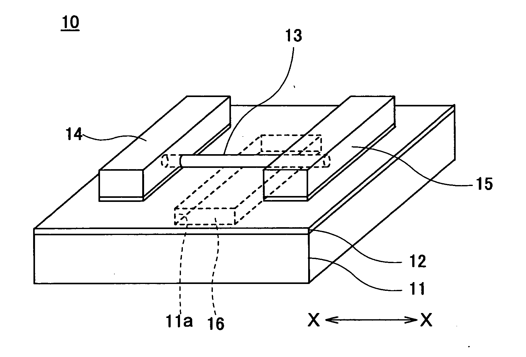
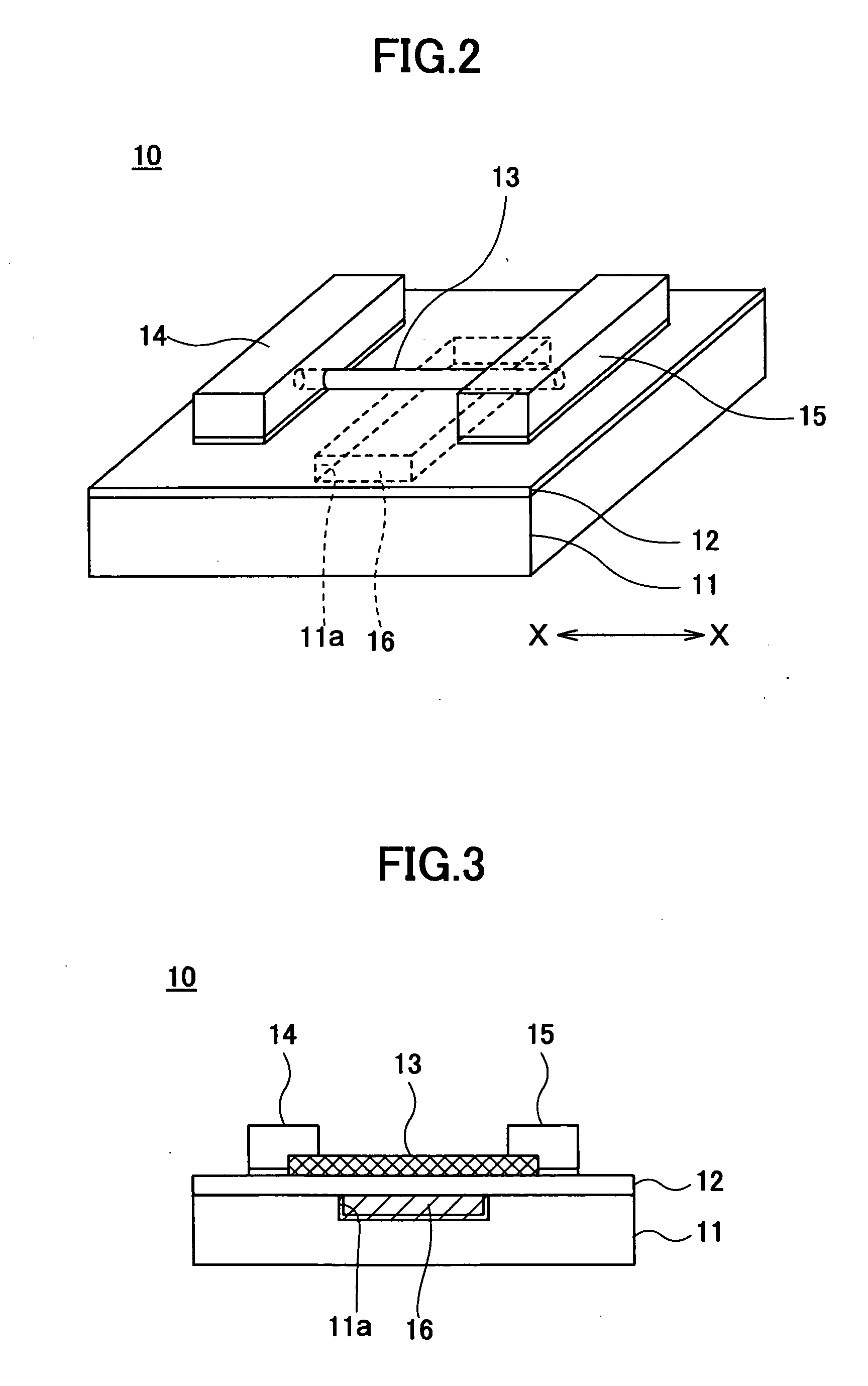
[0035]FIG. 2 shows a perspective view of a semiconductor device according to the first embodiment of the present invention, and FIG. 3 shows an elevational sectional view of the semiconductor device shown in FIG. 2 taken along an X direction.

[0036] As shown in FIGS. 2 and 3, the semiconductor device 10 according to the first embodiment of the present embodiment includes a substrate 11, a gate electrode 16 formed in a groove 11a formed in a surface of the substrate 11, a gate insulating film 12 covering a surface of the. substrate 11 and the gate electrode 16, a carbon nanotube 13 formed on the gate insulating film 12 in such a manner that a length direction of the gate electrode 16 coincides with a longitudinal direction (the X direction shown) of the carbon nanotube 13, and a source electrode 14 and a drain electrode 15 formed apart from one another along the longitudinal direction of the carbon nanotube 13 and in contact with the carbon n...

second embodiment

[0063] the present invention is described next.

[0064]FIG. 6 shows an elevational sectional view of a semiconductor device in a second embodiment of the present invention. In the figure, the same reference numerals are given to parts corresponding to those described above for the first embodiment, and duplicated description is omitted.

[0065] As shown in FIG. 6, the semiconductor device 30 according to the second embodiment includes a substrate 11, a gate electrode 31 formed on a surface of the substrate 11, a gate insulating film 32 covering the surface of the substrate 11 and the gate electrode 31, a carbon nanotube 13 formed on the gate insulating film 32 in such a manner that the length direction of the gate electrode coincides with the longitudinal direction of the carbon nanotube 13, and a source electrode 14 and a drain electrode 15 formed on the gate insulating film 32 apart from one another in the longitudinal direction of the carbon nanotube 13 and electrically connected wi...

third embodiment

[0071] the present invention is described next.

[0072]FIG. 7 shows an elevational sectional view of a semiconductor device in a third embodiment of the present invention. In the figure, the same reference numerals are given to parts corresponding to those described above for the first and second embodiments, and duplicated description is omitted.

[0073] As shown in FIG. 7, the semiconductor device 40 according to the third embodiment includes a substrate 11, a gate electrode 16 formed in a groove 11a formed in a surface of the substrate 11, a high dielectric gate insulating film 41 formed on the gate electrode 16, an insulating film 42 formed on the substrate 11 surface except the area of the gate electrode 16, a carbon nanotube 13 formed on the high dielectric gate insulating film 41 and the insulating film 42 in such a manner that the length direction of the gate electrode coincides with the longitudinal direction of the carbon nanotube 13, and a source electrode 14 and a drain ele...


PUM

PropertyMeasurementUnit
lengthaaaaaaaaaa
thicknessaaaaaaaaaa
thicknessaaaaaaaaaa

Abstract

A semiconductor device includes a substrate; a gate electrode formed on the substrate; a gate insulating film covering the gate electrode; a carbon nanotube disposed above the gate electrode and coming in contact with the gate insulating film; and a source electrode and a drain electrode formed apart from one another in a longitudinal direction of the carbon nanotube.

Description

BACKGROUND OF THE INVENTION [0001] 1. Field of the Invention [0002] The present invention relates to a semiconductor device having a channel made of a carbon nanotube, and a semiconductor sensor basically employing the same concept. [0003] 2. Description of the Related Art [0004] Operation speed in a semiconductor device such as a field effect transistor (FET) is increased by means of miniaturization, i.e., shortening of a gate length and reducing of a thickness of a gate insulating film. However, it is said that a hyperfine structure technology in an FET employing a silicon substrate almost has a limitation on a line width of tens of nanometers. [0005] In order to further increase operation speed in an FET, a carbon nanotube which enables high speed electron conduction has taken an attention. [0006] The carbon nanotube has a single dimensional shape having a diameter approximately in a range between several nanometers and ten nanometers, and a length of several micrometers, and the...

Claims


Application Information

Patent Timeline
Patent Type & Authority Applications(United States)
IPC IPC(8): B82B3/00B82B1/00G01N27/414H01L21/336H01L29/06H01L29/76H01L29/786H01L51/00H01L51/30
CPCB82Y10/00G01N27/4146H01L51/0545H01L51/0052H01L51/0048H10K85/221H10K85/615H10K10/466
Inventor HORIBE, MASAHIROHARADA, NAOKIYAMAGUCHI, YOSHITAKA
Owner FUJITSU LTD
Why Eureka
Try Eureka