Scribing sapphire substrates with a solid state UV laser

Inactive Publication Date: 2005-09-29
NEW WAVE RES
View PDF63 Cites 8 Cited by
  • Summary
  • Abstract
  • Description
  • Claims
  • Application Information

AI Technical Summary

Benefits of technology

[0009] The present invention provides a method and system for manufacturing integrated device die, such as diode laser die, from a sapphire substrate carrying an array of such integrated devices. Particularly, the present invention is suitable for manufacturing blue laser diodes based on gallium nitride structures. According to the present invention, greater density and greater yield are achieved, while also reducing the time required to separate the individual die from the substrate. Furthermore, the present invention is based on compact, low-cost machines, and otherwise reduces the overall manufacturing costs for such integrated device die.
[0011] Embodiments of the present invention produce laser pulses having an energy density between about 10 and 100 joules per square centimeter, a pulse duration between about 10 and 30 nanoseconds, and a spot size between about 5 and 25 microns. The repetition rate for the pulses is greater than 5 kHz, and preferably ranges from about 10 kHz to 50 kHz or higher. The stage is moved at a rate of motion causing overlap of the pulses in the amount of 50 to 99 percent. By controlling the pulse rate, the rate of motion of the stage, and the energy density, the depth of the scribe line can be precisely controlled. In embodiments of the invention, the scribe lines are cut to a depth of about one-half the thickness, or more, of the sapphire substrate, so that for an 80 micron thick substrate, the scribe line is cut to a depth in the range of about 35 microns to, for example, 60 microns, and more preferably greater than 40 microns.
[0013] In embodiments of the invention, the method includes detecting edges of the sapphire substrate while directing pulses at the substrate in the scribe pattern. In response to detected edges, the system prevents the pulses of radiation from being directed off of the substrate.
[0014] Embodiments of the present invention direct the pulses of radiation at the backside of the substrate. This prevents damage potentially caused by heat from reaching the active integrated device die structures. Furthermore, it prevents debris from the ablation process from contaminating the integrated devices on the die.
[0015] Thus, embodiments of the invention include placing the top surface of the substrate on an adhesive tape prior to scribing, mounting the substrate with the adhesive tape on the stage, moving the substrate under conditions causing ablation of the sapphire in a scribe pattern on the backside of the substrate, and detecting edges of the substrate during the scribing process to prevent the pulses of radiation from impacting the adhesive tape.
[0017] Embodiments of the invention further provide for controlling polarization of the laser pulses with respect to direction of scribe lines in the scribe pattern. The polarization is controlled so that the grooves are more uniform for scribe lines parallel to different axes. Uniformity can be improved by random or circular polarization of the pulses in some embodiments. More preferably, polarization of the pulse is controlled so that the polarization is linear and parallel to the scribe line being cut. It is found that the quality of the groove being formed is more V-shaped with parallel polarization, and more U-shaped with polarization that is not aligned. V-shaped grooves are preferred for more uniform and predictable breaking of the substrate during separation of the die. Embodiments of the invention provide for control of the polarization using a laser with an adjustable polarizer, such as a half wave plate, in the optical path.

Problems solved by technology

One bottleneck in manufacturing of die on sapphire substrates is the separation of the die from the substrate.
One major bottleneck in the manufacturing of the die is the cutting process.
In addition, the diamond tip blade must be operated relatively slowly, requiring as much as 1 and a half hours for a 2 inch diameter substrate.
Also, the diamond tips on the blade wear out and must be replaced often, as much as one blade per wafer.
Finally, the mechanical scribing process causes cracks, which can damage the die and reduce yields.

Method used


Image

  • Scribing sapphire substrates with a solid state UV laser
  • Scribing sapphire substrates with a solid state UV laser
  • Scribing sapphire substrates with a solid state UV laser

Examples


Embodiment Construction

[0030] A detailed description of embodiments of the present invention is provided with reference to FIGS. 1 through 8A-8C, and experimental results are shown in FIGS. 9-16.

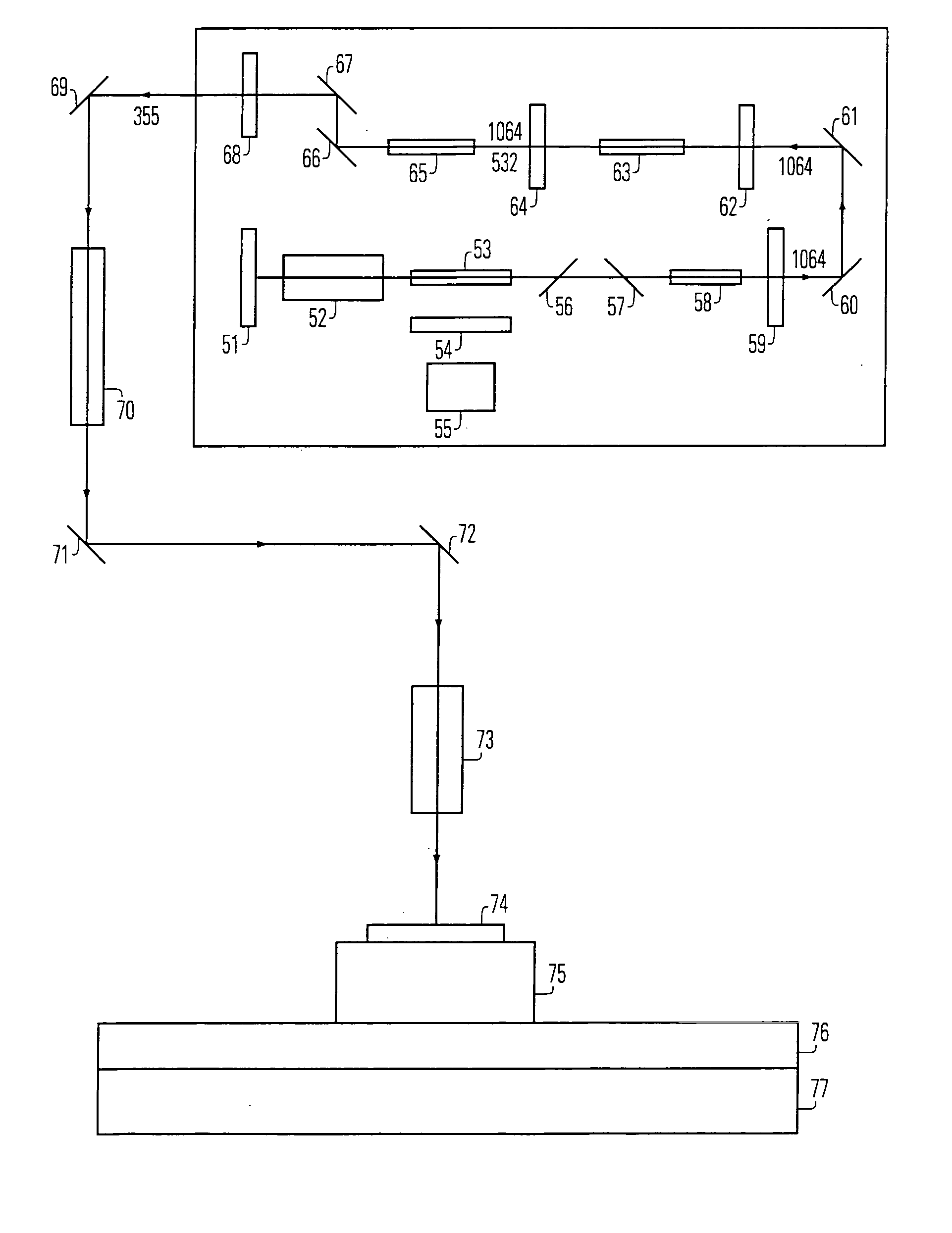
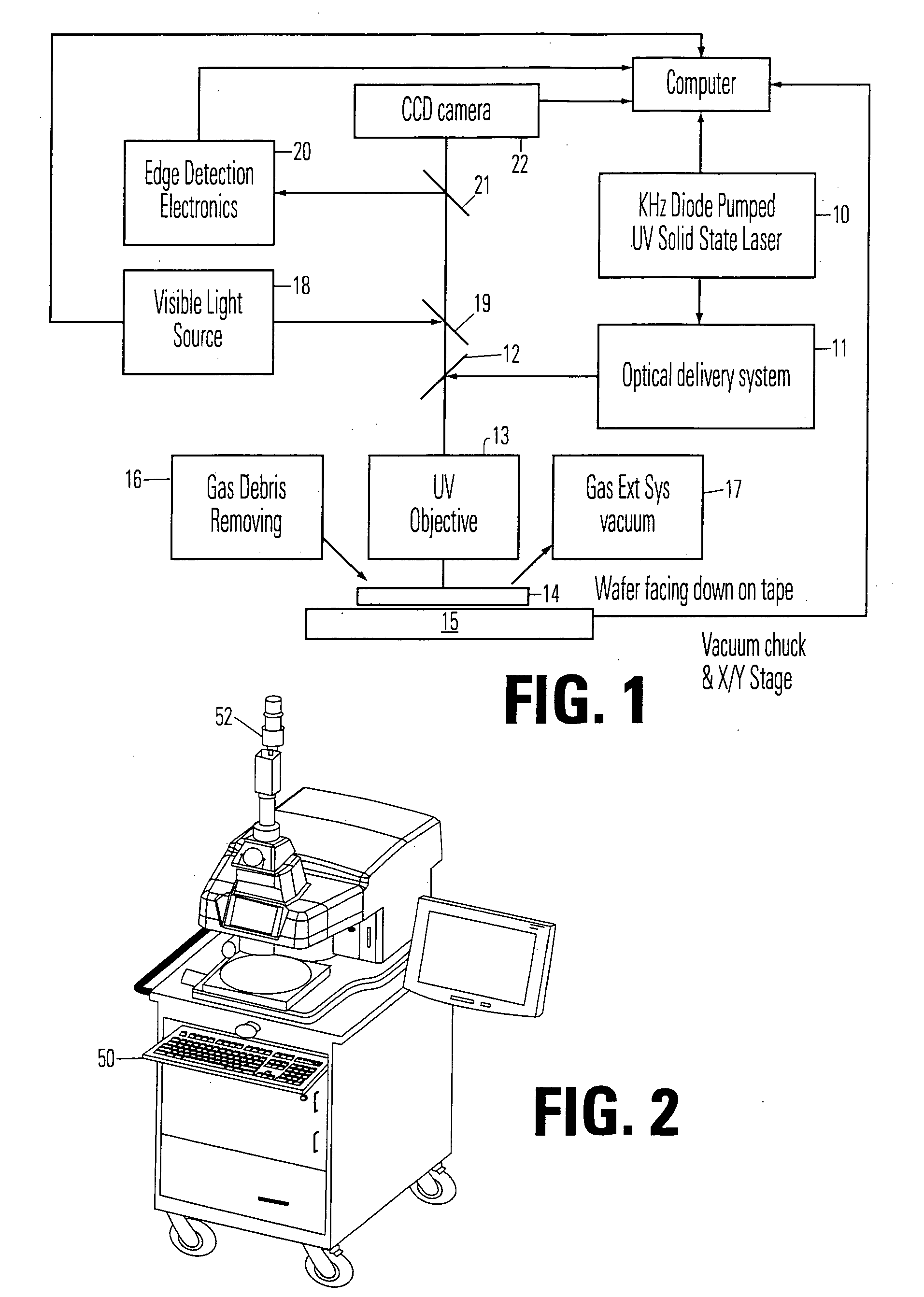
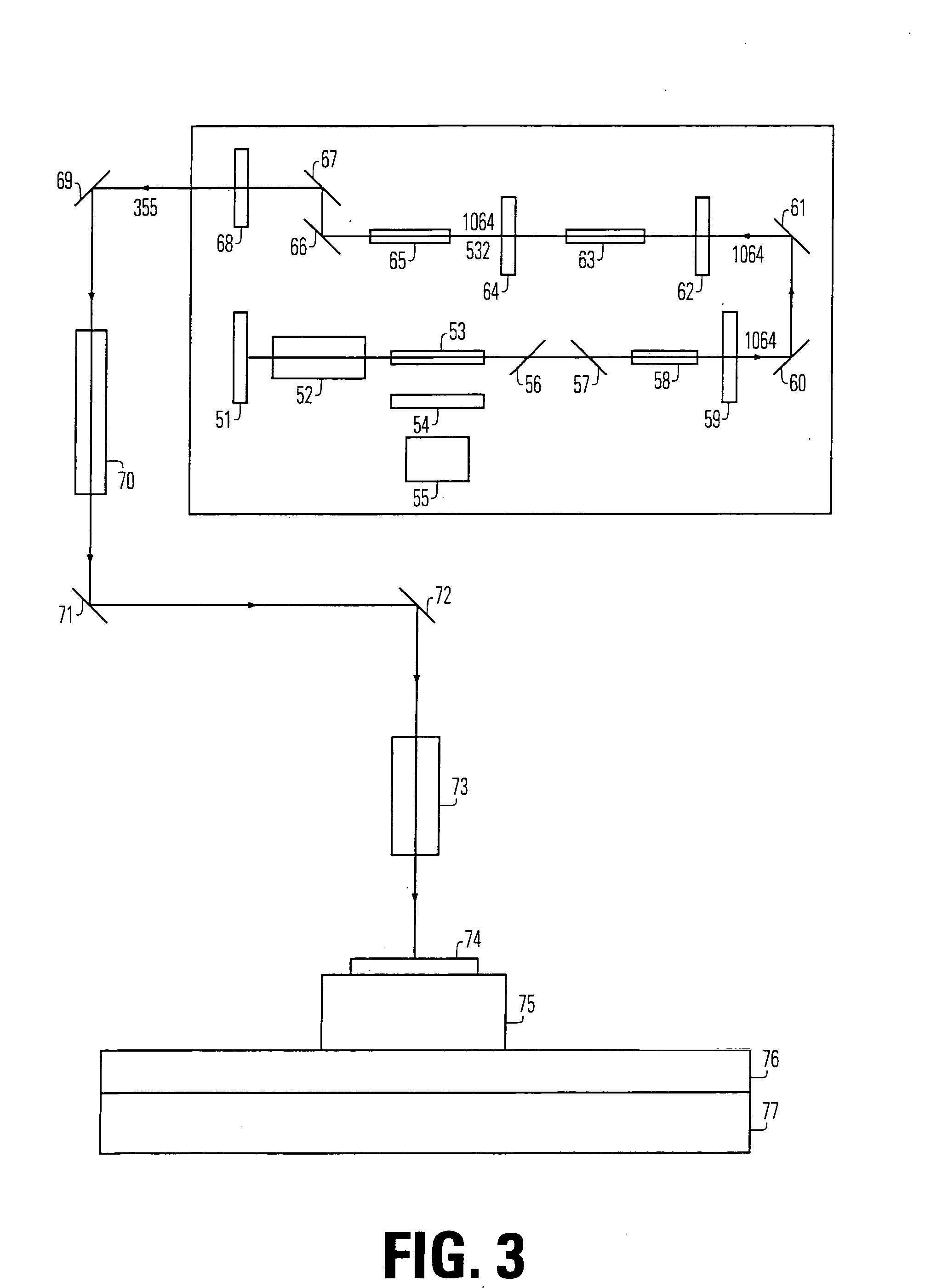
[0031]FIG. 1 is a simplified block diagram of a sapphire scribing system according to the present invention. In the embodiment shown, a diode pumped, solid-state laser 10 generates high-density UV and close-to-UV pulses at a repetition rate in the kHz range. In preferred systems, the laser comprises a Q-switched Nd:YVO4 medium delivering third harmonic output as the stream of laser pulses at a repetition rate greater than 10 kHz, with a pulse duration of about 40 nanoseconds. The pulses are provided using an optical delivery system 11 and turning mirror 12 to an ultraviolet objective lens 13, which focuses the pulses on a sapphire substrate 14. The substrate 14 is supported on a vacuum chuck and X / Y stage 15. Preferably, the wafer is supported face down on an adhesive wafer tape. A gas debris removing system 16 c...


PUM

PropertyMeasurementUnit
Lengthaaaaaaaaaa
Lengthaaaaaaaaaa
Sizeaaaaaaaaaa

Abstract

A process and system scribe sapphire substrates, by performing the steps of mounting a sapphire substrate, carrying an array of integrated device die, on a stage such as a movable X-Y stage including a vacuum chuck; and directing UV pulses of laser energy directed at a surface of the sapphire substrate using a solid-state laser. The pulses of laser energy have a wavelength below about 560 nanometers, and preferably between about 150 in 560 nanometers. In addition, energy density, spot size, and pulse duration are established at levels sufficient to induce ablation of sapphire. Control of the system, such as by moving the stage with a stationary beam path for the pulses, causes the pulses to contact the sapphire substrate in a scribe pattern at a rate of motion causing overlap of successive pulses sufficient to cut scribe lines in the sapphire substrate.

Description

RELATED APPLICATION DATA [0001] This application is a continuation of pending application Ser. No. 10 / 384,439, filed 6 Mar. 2003, which is a continuation of application Ser. No. 10 / 208,484, filed 30 Jul. 2002, now U.S. Pat. No. 6,580,054, which application claims the benefit of Provisional Application No. 60 / 387,381, filed 10 Jun. 2002. This application is related to application Ser. No. 10 / 364,587 filed 11 Feb. 2003.BACKGROUND OF THE INVENTION [0002] 1. Field of the Invention [0003] The present invention relates to systems and processes used in manufacturing integrated device die, such as integrated circuit and laser die, including diode laser die, formed on sapphire substrates. More particularly, the present invention provides for scribing sapphire substrates using solid state UV lasers, and separating the scribed sapphire substrate into die. [0004] 2. Description of Related Art [0005] Sapphire Al2O3 is used as a substrate for a variety of devices. The sapphire is a hard material ...

Claims


Application Information

Patent Timeline
IPC IPC(8): B23K26/03B23K26/08B23K26/38B23K101/40B28D5/00H01L21/324H01L21/477H01L21/78H01L33/00H01S3/00H01S5/02H01S5/323
CPCB23K26/03B23K26/032B23K26/063B23K26/073B23K26/367B23K26/4045H01S5/32341B23K2201/40B28D5/0011H01L21/78H01L33/0095H01S5/0201H01S5/0213B23K26/4075B23K26/364B23K26/0622B23K26/40B23K2103/36B23K2103/50B23K2101/40
Inventor LIU, KUO-CHINGFANG, PEI HSIENDERE, DANLIU, JENNHUANG, JIH-CHUANGLUCERO, ANTONIOPINKHAM, SCOTTOLTROGGE, STEVENMIDDLEBUSHER, DUANE
Owner NEW WAVE RES
Why Eureka
Try Eureka