Fixture and method for uniform electroless metal deposition on integrated circuit bond pads

a technology of electroless plating and bonding pads, which is applied in the direction of liquid/solution decomposition chemical coating, semiconductor/solid-state device details, coatings, etc., can solve the problems of significant technological challenges, pronounced aluminum sensitivity to electromigration becoming a serious obstacle, and the need for expensive photolithographic definition steps. to avoid the effect of expensive photolithographic definition steps

Inactive Publication Date: 2005-10-06
AMADOR GONZALO +1
View PDF8 Cites 4 Cited by
  • Summary
  • Abstract
  • Description
  • Claims
  • Application Information

AI Technical Summary

Benefits of technology

[0012] It is an aspect of the present invention to be applicable to bond pad area reduction and thus to be in support of the shrinking of IC chips. Consequently, the invention helps to alleviate the space constraint of continually shrinking applications such as cellular communication, pagers, hard disk drives, laptop computers and medical instrumentation.
[0013] Another aspect of the invention is to deposit the bond pad metal caps by the self-defining process of electroless plating, thus avoiding costly photolithographic and alignment techniques.
[0015] Another aspect of the invention is to advance the process and reliability of wafer-level multi-probing by eliminating probe marks and subsequent bonding difficulties.
[0017] Another object of the invention is to use only designs and processes most commonly employed and accepted in the fabrication of IC devices, thus avoiding the cost of new capital investment and using the installed fabrication equipment base.
[0019] In the first embodiment of the invention, an apparatus is disclosed for uniform electroless plating of layers onto exposed metallizations in integrated circuits, such as bond pads, which are positioned on the active surface of semiconductor wafers. The apparatus is suitable for simultaneous processing of a plurality of wafers. It provides rotation at constant speed synchronously to the wafers and thus creates relative motion, between the wafers and the chemical solution of a plating bath.
[0021] In all preferred embodiments, the various metal layers are deposited by electroless plating, thus avoiding the need for expensive photolithographic definition steps.

Problems solved by technology

Consequently, the relatively high resistivity of the interconnecting aluminum now appears inferior to the lower resistivity of metals such as copper.
Further, the pronounced sensitivity of aluminum to electromigration is becoming a serious obstacle.
From the standpoint of the mature aluminum interconnection technology, however, this shift to copper is a significant technological challenge.
For bond pads made of copper, the formation of thin copper(I)oxide films during the manufacturing process flow has to be prevented, since these films severely inhibit reliable attachment of bonding wires, especially for conventional gold-wire ball bonding.
In contrast to aluminum oxide films overlying metallic aluminum, copper oxide films overlying metallic copper cannot easily be broken by a combination of thermocompression and ultrasonic energy applied in the bonding process.
As further difficulty, bare copper bond pads are susceptible to corrosion.
First, the fabrication cost of the aluminum cap is higher than desired, since the process requires additional steps for depositing metal, patterning, etching, and cleaning.
Second, the cap must be thick enough to prevent copper from diffusing through the cap metal and possibly poisoning the IC transistors.
Third, the aluminum used for the cap is soft and thus gets severely damaged by the markings of the multiprobe contacts in electrical testing.
This damage, in turn, becomes so dominant in the ever decreasing size of the bond pads that the subsequent ball bond attachment is no longer reliable.
The structure provides a metal layer plated onto the copper, which impedes the up-diffusion of copper.
This layer is topped by a bondable metal layer, which also impedes the up-diffusion of the barrier metal.
It is difficult, though, to plate these bond pad caps uniformly in electroless deposition systems, because electroless deposition is affected by local reactant concentrations and by the agitation velocities of the aqueous solution.
Increasing the agitation of the solution only exacerbates the deposition non-uniformity, which is influenced by the flow direction of the solution.
The problem is further complicated when a whole batch of wafers is to be plated simultaneously in order to reduce cost, since known control methods have been applied only to process single wafers under applied electrical bias.

Method used


Image

  • Fixture and method for uniform electroless metal deposition on integrated circuit bond pads
  • Fixture and method for uniform electroless metal deposition on integrated circuit bond pads
  • Fixture and method for uniform electroless metal deposition on integrated circuit bond pads

Examples


first embodiment

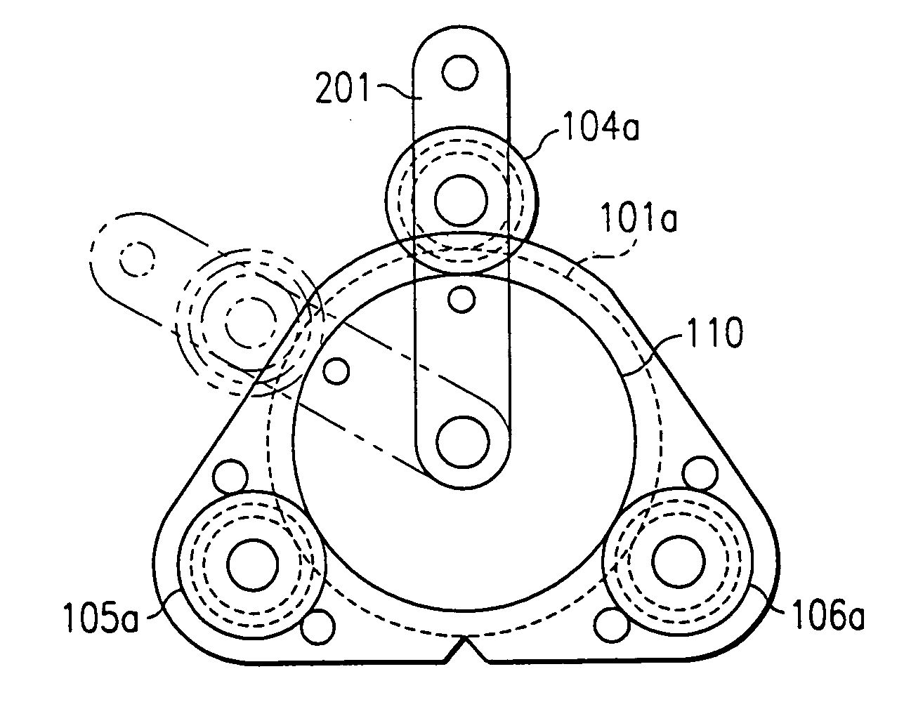
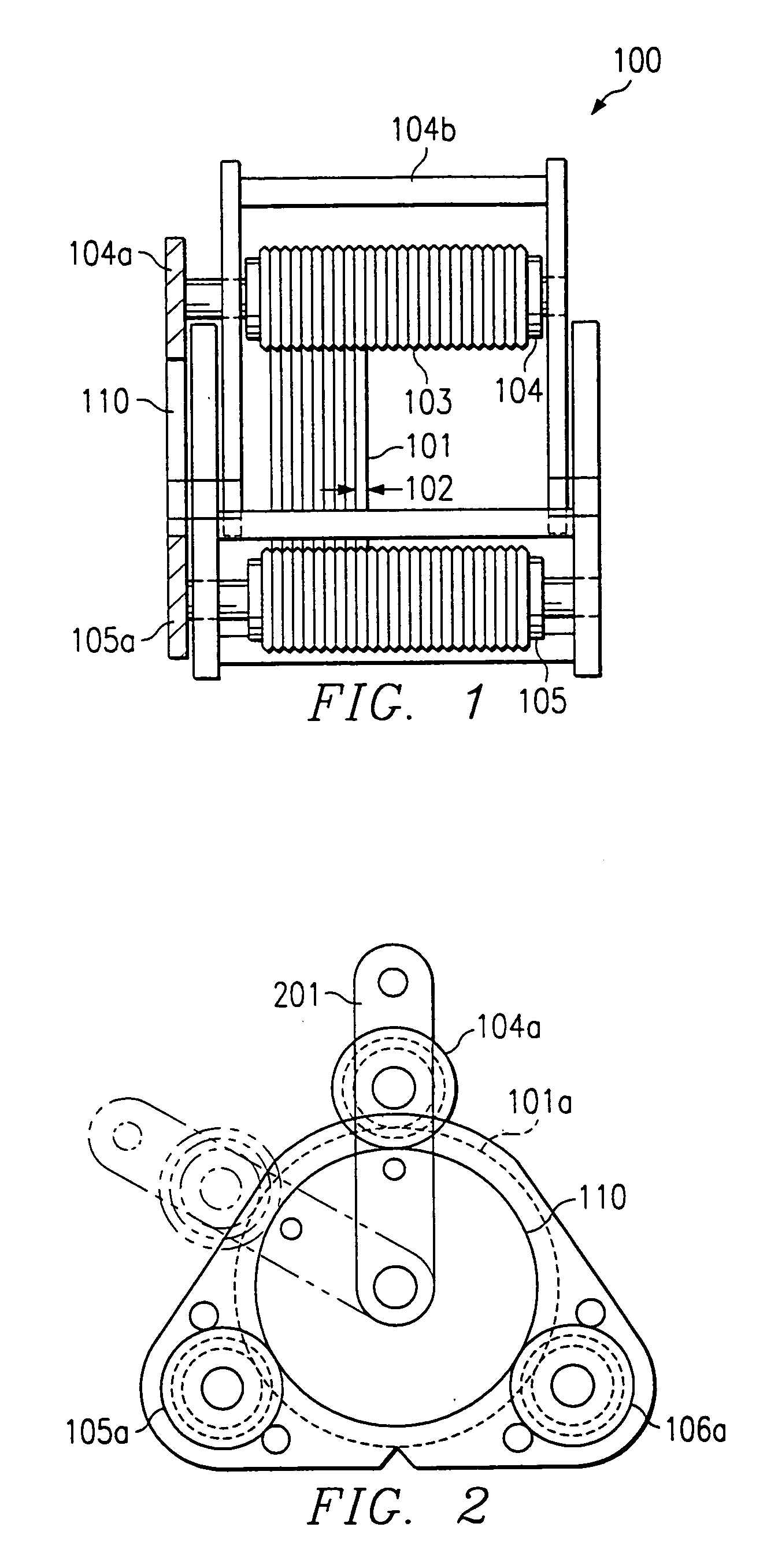
[0027] Illustrating the invention, generally designated 100, FIG. 1 shows a side view of the apparatus for controlled electroless plating of uniform metal layers onto exposed metallizations on a plurality of integrated circuit (IC) wafers 101. Usually, there are 10 to 30 wafers in a batch. In the fixture 100, the wafers 101 are held approximately parallel to each other at predetermined distances 102. A typical distance is in the range from about 5 to 10 mm and thus several times wider than the thickness of a wafer (about 0.25 to 0.75 mm). At their rims, the wafers are loosely held in grooves 103 of rollers. In FIG. 1, two rollers are shown, the bottom roller 105 and the capture roller 104. The rollers are made of chemically inert plastic material such as polypropylene. Instead of grooved rollers, toothed rollers may be used. A practical groove is about 2 to 5 mm deep. In the preferred embodiments, there are three rollers (see FIG. 2) employed to contain the wafers.

[0028] It is an es...

second embodiment

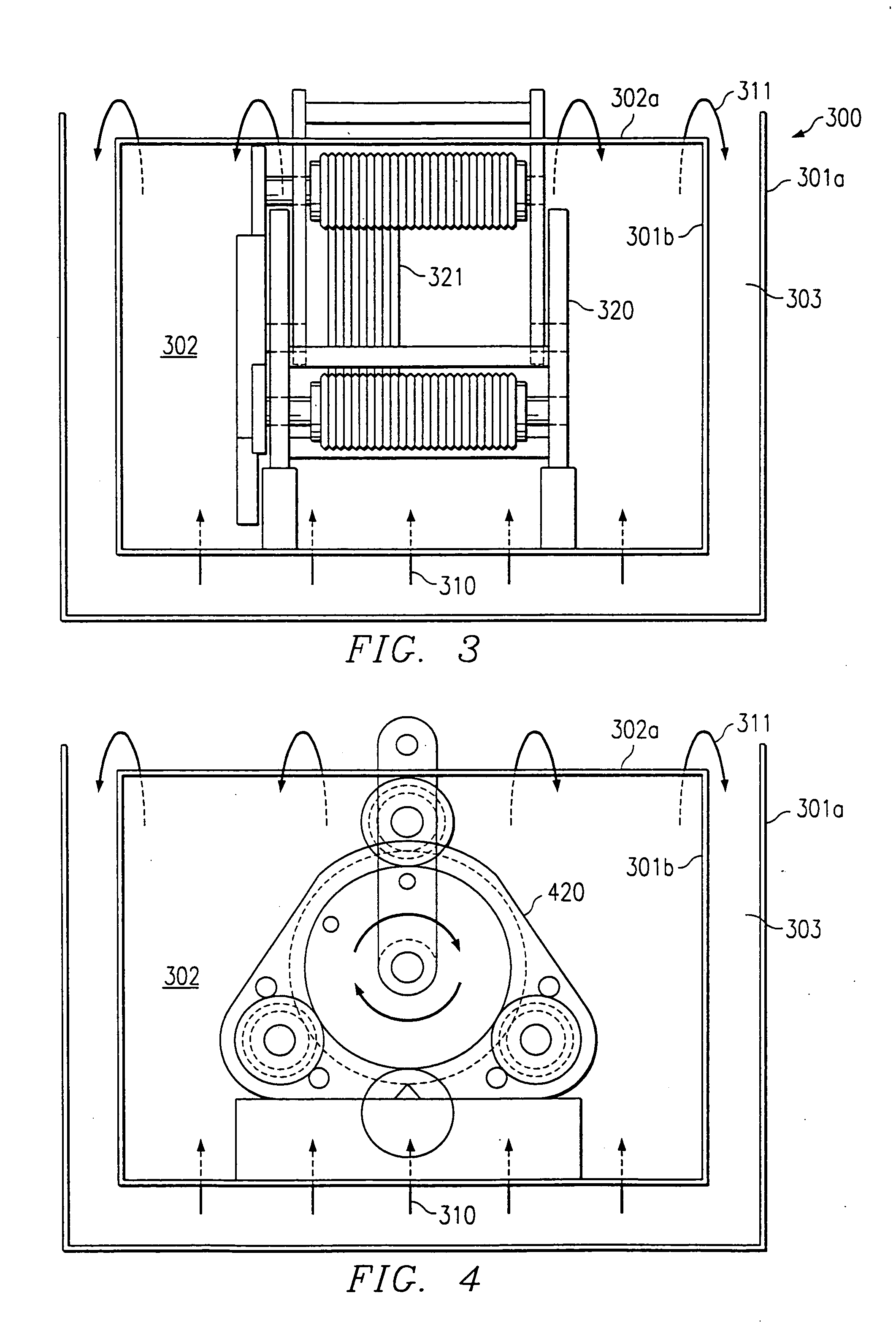
[0030] Illustrating the invention, generally designated 300, as well as the process for electroless plating, FIGS. 3 and 4 show schematically the cross section through a plating tank filled by the liquid plating solution 302 up to the surface 302a of the solution. The plating tank has an outer wall 301a and an inner wall 301b, separated by a gap 303, which enables the reflow of the liquid. In FIGS. 3 and 4, arrows indicate the flow of the liquid solution. As can be seen, the solution enters the tank from the bottom (arrows 310), moves in laminar flow at constant speed upward (for example, at a speed of 20 cm / min) through the tank, and exits from the tank surface (arrows 311) by overflowing into the reflow gap 303. After reaching the tank bottom, the flow cycle begins anew.

[0031] Further shown in FIGS. 3 and 4 is the apparatus / fixture for holding a plurality of wafers, explained in FIGS. 1 and 2. In FIG. 3, the fixture is illustrated in side view 320 as in FIG. 1; in FIG. 4, the fixt...


PUM

PropertyMeasurementUnit
thicknessaaaaaaaaaa
thicknessaaaaaaaaaa
speedaaaaaaaaaa

Abstract

A method and an apparatus for uniform electroless plating of layers onto exposed metallizations in integrated circuits such as bond pads. The apparatus provides means for holding a plurality of wafers, and rotating each wafer at constant speed and synchronous within the plurality. Immersed in a plating solution flowing in substantially laminar motion and at constant speed, the method creates periodic superposition of directions and speeds of the motion of the wafers and the motion of the plating solution. The invention creates periodically changing wafer portions where the directions and speeds are additive and where the directions and speeds are opposed and subtractive. Consequently, highly uniformly layers are electrolessly plated onto the exposed metallizations of bond pads. If the plated layers are bondable metals, the process transforms otherwise unbondable pad metallization into bondable pads.

Description

FIELD OF THE INVENTION [0001] The present invention is related in general to the field of semiconductor devices and processes and more specifically to a fixture and process for electroless plating bondable metal caps onto bond pads of integrated circuits having copper interconnecting metallization. DESRCIPTION OF THE RELATED ART [0002] In integrated circuits (IC) technology, pure or doped aluminum has been the metallization of choice for interconnection and bond pads for more than four decades. Main advantages of aluminum include ease of deposition and patterning. Further, the technology of bonding wires made of gold, copper, or aluminum to the aluminum bond pads has been developed to a high level of automation, miniaturization, and reliability. Examples of the high technical standard of wire bonding to aluminum can be found in U.S. Pat. No. 5,455,195, issued on Oct. 3, 1995 (Ramsey et al., “Method for Obtaining Metallurgical Stability in Integrated Circuit Conductive Bonds”); U.S. ...

Claims


Application Information

Patent Timeline
Patent Type & Authority Applications(United States)
IPC IPC(8): C23C18/16C23C18/31C23C18/36H01L21/288H01L21/3205H01L21/60H01L23/52
CPCC23C18/1619H01L2224/0401H01L21/288H01L24/02H01L24/11H01L2224/04042H01L2224/13099H01L2924/01004H01L2924/01006H01L2924/01011H01L2924/01013H01L2924/01014H01L2924/01029H01L2924/01033H01L2924/01046H01L2924/01075H01L2924/01078H01L2924/01079H01L2924/01327H01L2924/14H01L2924/3025C23C18/1669H01L24/05H01L2224/45124H01L2224/45144H01L2224/45147H01L2924/00011H01L2924/00H01L2924/00014
Inventor AMADOR, GONZALOSTIERMAN, ROGER J.
Owner AMADOR GONZALO
Why Eureka
Try Eureka