4H-polytype gallium nitride-based semiconductor device on a 4H-polytype substrate

a gallium nitride-based semiconductor and polytype technology, applied in semiconductor devices, semiconductor lasers, semiconductor lasers, etc., can solve the problem of unclear crystal quality

Inactive Publication Date: 2005-10-06
PANASONIC CORP
View PDF3 Cites 39 Cited by
  • Summary
  • Abstract
  • Description
  • Claims
  • Application Information

AI Technical Summary

Problems solved by technology

Due to the difficulties to obtain lattice-matched III-V nitride substrates, conventional III-V nitride devices are grown on foreign substrates such as sapphire or SiC.
However, how the combination of the polytype of SiC substrate and that of the overgrown III-V nitrides affect the crystal quality is not still clear.

Method used


Image

  • 4H-polytype gallium nitride-based semiconductor device on a 4H-polytype substrate
  • 4H-polytype gallium nitride-based semiconductor device on a 4H-polytype substrate
  • 4H-polytype gallium nitride-based semiconductor device on a 4H-polytype substrate

Examples


first embodiment

[0030] (Device Structure)

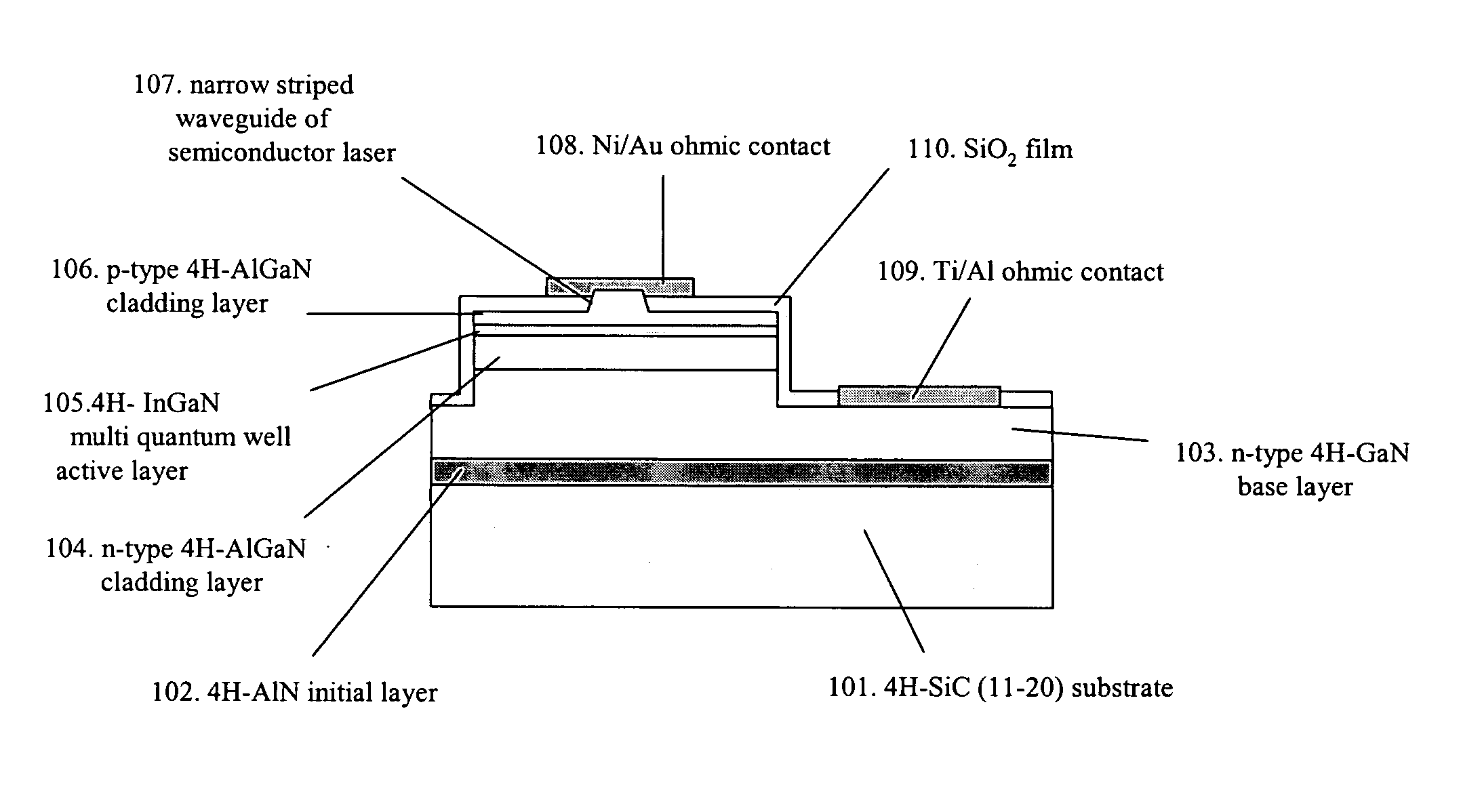
[0031] Referring first to FIG. 1, one embodiment of the semiconductor laser of the present invention may be understood in greater detail. In particular, FIG. 1 schematically illustrates a cross sectional view of a blue-violet semiconductor laser in which GaN-based epitaxial structure with 4H polytype is grown on (11-20) a-face of 4H-SiC substrate. The GaN-based epitaxial structure typically consists of p-type Al0.07Ga0.93N cladding layer 106, undoped InGaN multi quantum well active layer 105, n-type Al0.07Ga0.93N cladding layer 104 and n-type GaN base layer 103 And the undoped InGaN multi quantum well active layer 105 is disposed between the p-type AlGaN cladding layer 106 and n-type AlGaN cladding layer 104, and these three layers are formed on the n-type GaN base layer 103 as shown in FIG. 1. Moreover, n-type GaN base layer 103 is formed on the undoped AlN initial layer 102. All of the epitaxial layers have 4H poly type and the layers are grown replicatin...

second embodiment

[0056] Referring next to FIG. 12, there is schematic illustration of a non-polar GaN based blue-violet semiconductor laser on a 4H-SiC (11-20) a-face substrate 1201. Basic epitaxial structures on 4H-SiC (11-20) a-face is identical with the structure as shown in FIG. 1. However, dislocation density in the active layer underneath the waveguide 1208 is further reduced by employing the epitaxial lateral over growth technique. The resultant laser exhibits longer lifetime than that without any lateral growth region owing to the reduction of the dislocations. The emission efficiency from the quantum well in the laser is increased from that on the polar c-face with built-in electric field due to the polarization, which leads to lower threshold current density.

[0057] As shown in FIG. 12, the epitaxial structure of the laser typically consists of an undoped InGaN multi quantum well active layer 1206 formed between a p-type Al0.07Ga0.93N cladding layer 1207 and an n-type Al0.07Ga0.93N claddin...

third embodiment

[0069] Referring next to FIG. 13(a) and (b), non-polar GaN-based blue-violet laser diodes on 4H-SiC (11-20) a-face substrates with two electrodes on the both sides of the laser chip are shown. Epitaxial structure on 4H-SiC (11-20) a-face is basically identical with the structure shown as the first embodiment except for the initial layer. In the first embodiment, the initial layer is AlN, however in this embodiment, the initial layer which is formed on the substrate 1301 is conductive AlGaN layer. And also in this embodiment, the 4H-SiC substrate 1301 is conductive to enable the vertical device configuration. The emission efficiency from the quantum well in the laser on the non polar face is increased from that on the polar c-face with built-in electric field due to the polarization, which leads to lower threshold current density together with low series resistance and operating voltage owing to its vertical device configuration.

[0070] As shown in FIG. 13(a) and (b), the epitaxial s...


PUM

PropertyMeasurementUnit
thicknessaaaaaaaaaa
thicknessaaaaaaaaaa
lengthaaaaaaaaaa

Abstract

4H-InGaAlN alloy based optoelectronic and electronic devices on non-polar face are formed on 4H-AlN or 4H-AlGaN on (11-20) a-face 4H-SiC substrates. Typically, non polar 4H-AlN is grown on 4H-SiC (11-20) by molecular beam epitaxy (MBE). Subsequently, III-V nitride device layers are grown by metal organic chemical vapor deposition (MOCVD) with 4H-polytype for all of the layers. The non-polar device does not contain any built-in electric field due to the spontaneous and piezoelectric polarization. The optoelectonic devices on the non-polar face exhibits higher emission efficiency with shorter emission wavelength because the electrons and holes are not spatially separated in the quantum well. Vertical device configuration for lasers and light emitting diodes(LEDs) using conductive 4H-AlGaN interlayer on conductive 4H-SiC substrates makes the chip size and series resistance smaller. The elimination of such electric field also improves the performance of high speed and high power transistors. The details of the epitaxial growth s and the processing procedures for the non-polar III-V nitride devices on the non-polar SiC substrates are also disclosed.

Description

FIELD OF THE INVENTION [0001] The present invention relates to semiconductor devices using 4H-polytype GaN-based nitride semiconductor epitaxial layers grown on 4H-polytype substrates, and more particularly relates to method for increasing emission efficiency of the GaN-based optoelectronic devices and enabling high speed and high power operations of the GaN-based electronic devices. BACKGROUND [0002] III-V nitrides are wide band gap III-V compound semiconductors which contain nitrogen as a group-V element, and generally written as B1-x-y-zInxAlyGazN (0≦x≦1, 0≦y≦1, 0≦z≦1). Such III-V nitrides are widely used for visible light emitting diodes (LEDs) in many applications such as various indicators, traffic signals and so on. In addition, excitation of fluorescent material using the GaN-based blue or ultraviolet LEDs enables emitting white light, which would replace current light bulbs with longer lifetime. A blue-violet GaN-based semiconductor lasers for high-density optical disk syst...

Claims


Application Information

Patent Timeline
Patent Type & Authority Applications(United States)
IPC IPC(8): H01L21/02H01L29/26H01L21/20H01L21/338H01L29/778H01L29/812H01L33/18H01L33/32H01S5/323
CPCH01L21/02082H01L21/02378H01L21/02433H01L21/02458H01L33/32H01L21/0262H01L21/02639H01L21/0265H01L33/18H01L21/0254
Inventor UEDA, TETSUZOKIMOTO, TSUNENOBUMATSUNAMI, HIROYUKISUDA, JUNONOJIMA, NORIO
Owner PANASONIC CORP
Why Eureka
Try Eureka