Metal-doped alumina and layers thereof

Inactive Publication Date: 2005-10-06
MICRON TECH INC
View PDF62 Cites 90 Cited by
  • Summary
  • Abstract
  • Description
  • Claims
  • Application Information

AI Technical Summary

Benefits of technology

[0007] This invention provides methods of forming a metal-doped aluminum oxide (i.e., alumina) layer on a substrate, particularly a semiconductor substrate or substrate assembly, using a vapor deposition technique. The methods involve forming the layer by combining one or more yttrium or lanthanide diketonate and/or ketoimine and/or organo-oxide precursor compounds with one or more aluminum precursor co

Problems solved by technology

The continuous shrinkage of microelectronic devices such as capacitors and gates over the years has led to a situation where the materials traditionally used in integrated circuit technology are approaching their performance limits.
However, when the SiO2 layer is thinned to 1 nm (i.e., a thickness of only 4 or 5 molecules), as is desired in the new

Method used


Image

  • Metal-doped alumina and layers thereof
  • Metal-doped alumina and layers thereof
  • Metal-doped alumina and layers thereof

Examples


Example

Example 1

Atomic Layer Deposition of (Y,Al)2O3

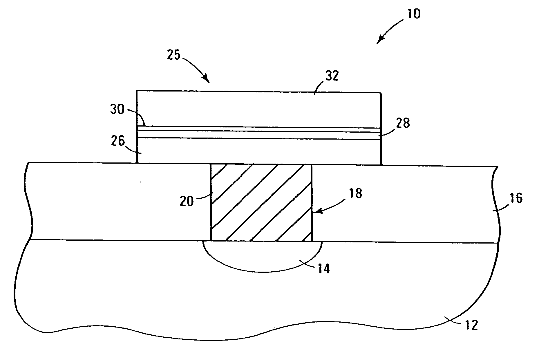
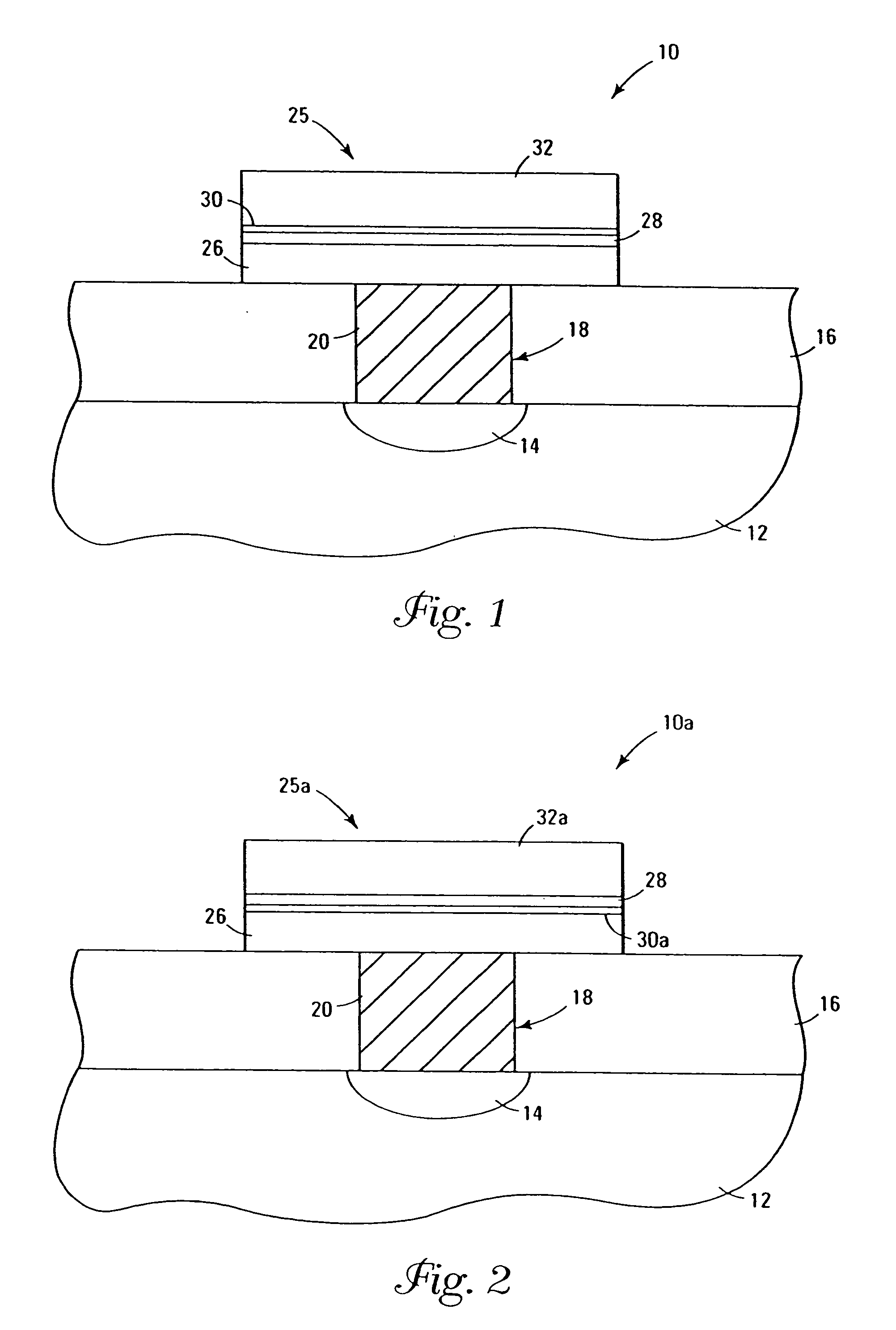
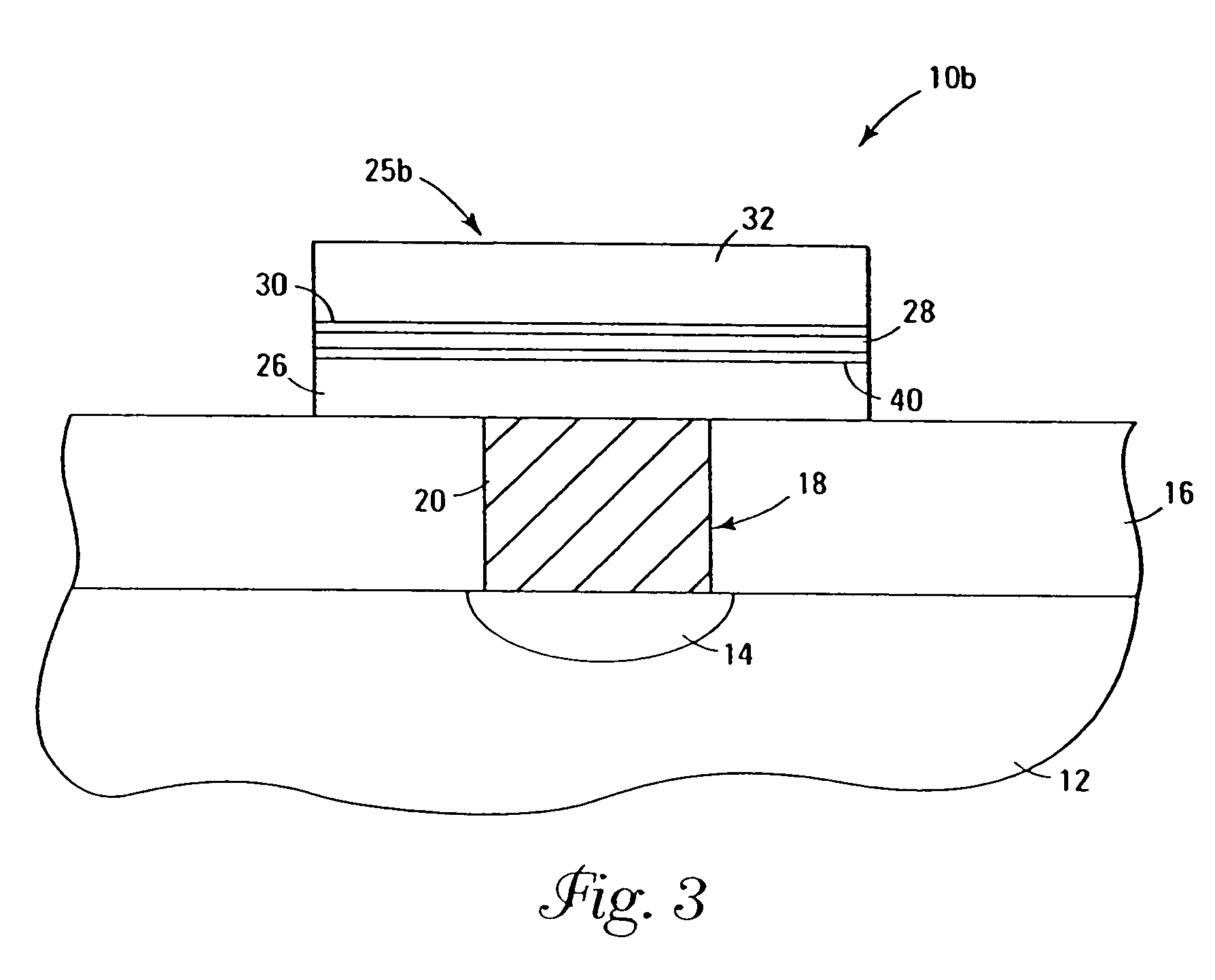
[0071] The deposition of (Y,Al)2O3 was carried out using alternating pulses of Y(thd)3 (available from Strem Chemical Co., Newburyport, Mass.) and Al(Et)3 (available from Rohm & Haas, Danvers, Mass.) vapor in an ALD process. The precursors were held at 190° C. and 50° C., respectively. The substrate had a top layer of 1500 Angstroms of doped polysilicon and was held at 300° C. during 400 cycles. The film formed was approximately 400 Angstroms thick and remained amorphous (as determined by XRD) even after a 750° C. anneal in nitrogen for 1 minute. The ratio of Yttrium to Aluminum was determined by XPS and further identified by ICP spectroscopy to have an approximate stoichiometry of Y0.1Al1.9O3. TEM showed an amorphous (Y,Al)2O3 with no apparent SiO2 at the interface. Electrical measurements were performed on the material by sputtering platinum electrodes on top of the film through a hard mask. The dielectric constant was 34 at 1 kHz and...


PUM

PropertyMeasurementUnit
Dielectric polarization enthalpyaaaaaaaaaa
Ratioaaaaaaaaaa

Abstract

A method of forming (and an apparatus for forming) a metal-doped aluminum oxide layer on a substrate, particularly a semiconductor substrate or substrate assembly, using a vapor deposition process.

Description

FIELD OF THE INVENTION [0001] This invention relates to methods of forming a metal-doped aluminum oxide layer on a substrate using one or more lanthanide precursor compounds that include one or more diketonate ligands and / or ketoimine ligands and / or organo-oxide ligands during a vapor deposition process. The precursor compounds and methods are particularly suitable for the formation of metal-doped aluminum oxide layers on semiconductor substrates or substrate assemblies. BACKGROUND OF THE INVENTION [0002] The continuous shrinkage of microelectronic devices such as capacitors and gates over the years has led to a situation where the materials traditionally used in integrated circuit technology are approaching their performance limits. Silicon (i.e., doped polysilicon) has generally been the substrate of choice, and silicon dioxide (SiO2) has frequently been used as the dielectric material with silicon to construct microelectronic devices. However, when the SiO2 layer is thinned to 1 ...

Claims


Application Information

Patent Timeline
IPC IPC(8): H01L21/316C23C16/40H01L21/3115H01L21/8244
CPCC23C16/40H01L21/02178H01L21/02192H01L21/02194H01L21/02205H01L21/0228H01L21/3115H01L21/3162H01L27/11H10B10/00
Inventor VAARTSTRA, BRIAN A.
Owner MICRON TECH INC
Why Eureka
Try Eureka