Semiconductor laser device

Active Publication Date: 2005-10-13
SHARP FUKUYAMA LASER CO LTD
View PDF6 Cites 39 Cited by
  • Summary
  • Abstract
  • Description
  • Claims
  • Application Information

AI Technical Summary

Benefits of technology

[0009] More specifically, according to the present invention, in the case of using a substrate having a refractive index ns larger than an effective refractive index ne in a waveguide region, a clad layer provided between the substrate and an active layer is divided into at least three layers and among the three clad layers a clad layer having the smallest refractive index is arranged between the other clad layers to r

Problems solved by technology

A laser device causing such a noise peak involves a problem in application to optical disks etc.
Further, such a noise peak corresponds to radiation loss of waveguide, involving problems of increase of threshold current in the laser device and decrease of differential quantum efficiency in lasing.
In that case, however, n-type Al

Method used


Image

  • Semiconductor laser device
  • Semiconductor laser device
  • Semiconductor laser device

Examples


first embodiment

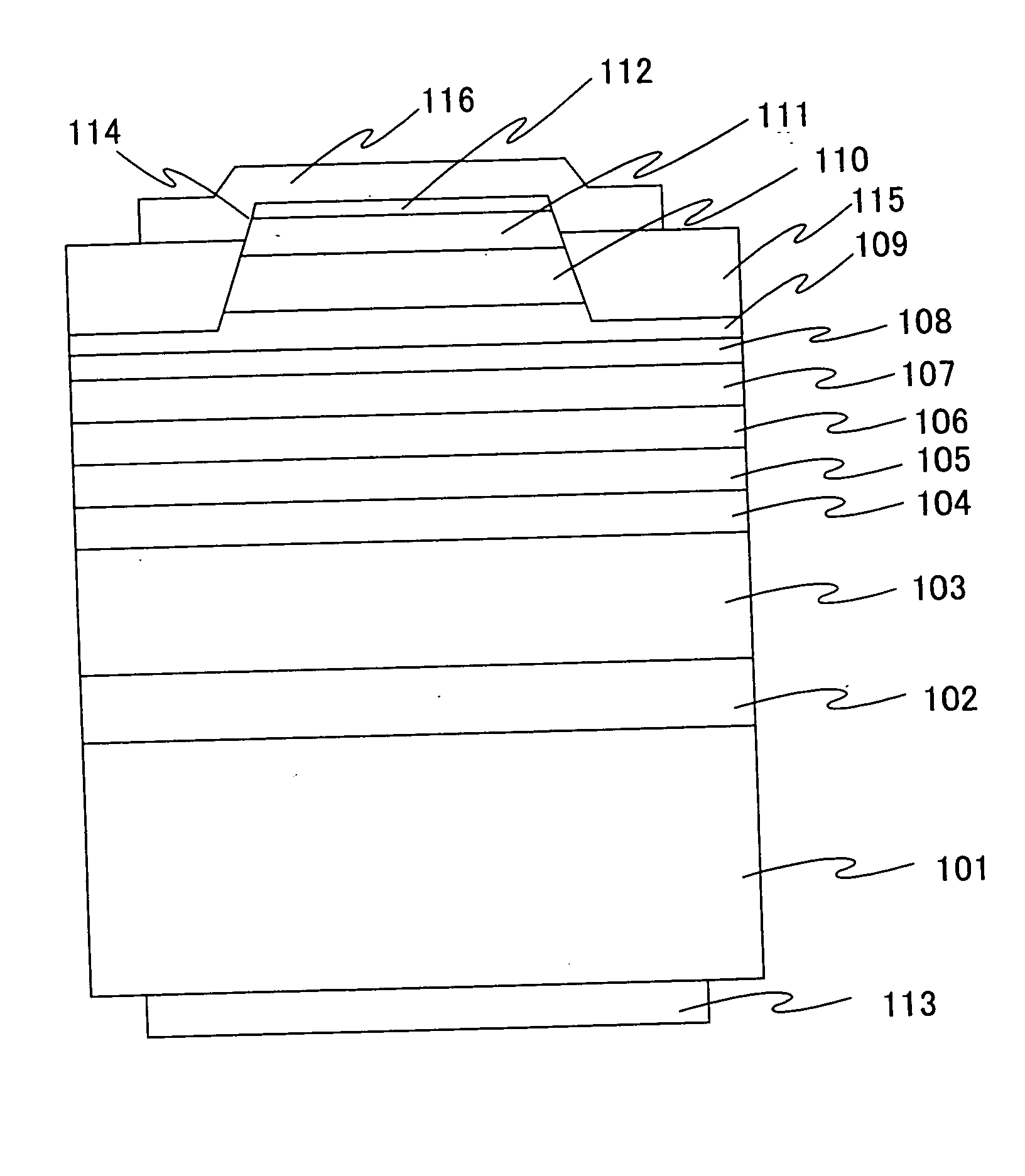
[0049] As a first embodiment, a process of fabricating the FIG. 1 nitride semiconductor laser device will be described. Initially, n-type GaN underlying layer 102 of 3 μm thickness is grown on n-type GaN substrate 101 at 1125° C., using hydrogen as a carrier gas, trymethylgallium (TMG) and ammonium as source gases, and silane (SiH4) as a dopant gas.

[0050] Then, at the same substrate temperature, hydrogen serving as a carrier gas, trymethy aluminum (TMA), TMG and ammonium serving as source gases, and silane serving as a dopant gas are used to grow first n-type clad layer 103 of Al0.05Ga0.95N doped with Si at a concentration of 3×1018 cm−3 to have a thickness of 1.8 μm. Similarly, second n-type clad layer 104 of Al0.1Ga0.9N doped with Si at a concentration of 3×1018 cm−3 is grown to a thickness of 0.2 μm. Similarly, third n-type clad layer 105 of Al0.05Ga0.95N doped with Si at a concentration of 3×1018 cm−3 is grown to a thickness of 0.1 μm.

[0051] Then, at the same substrate tempera...

second embodiment

[0062]FIG. 3 is a schematic front view of a laser device according to a second embodiment. As seen from FIG. 3 in comparison with FIG. 1, the second embodiment provides a laser device different from the first embodiment only in that a strain alleviation layer 120 is inserted between n-type underlying layer 102 and first n-type clad layer 103. Strain alleviation layer 120 can be made of n-type In0.09Ga0.91N for example.

[0063] More specifically, at a substrate temperature of 800° C., a gaseous mixture of nitrogen of 95% and hydrogen of 5% serving as a carrier gas, TMG, TMI and ammonium serving as source gases, and further, silane serving as a dopant gas can be used to form n-type In0.09Ga0.91N strain alleviation layer 120 doped with Si at a concentration of 5×1018 cm−3 to have a thickness of 0.03 μm.

[0064] The second embodiment provides an increased yield rate of 94% of the laser device which shows similar characteristics as in the first embodiment.

third embodiment

[0065] A third embodiment provides a laser device different from the first embodiment only in that dielectric layer 115 shown in FIG. 1 is replaced with a high-resistance or n-type AlGaN layer. Such a laser device of the third embodiment can bring about similar effects as in the first embodiment. The AlGaN layer can be deposited for example by MOVPE, MOCVD, HVPE, MBE, or other similar crystal growth technique. Furthermore, if sputtering is employed to deposit the AlGaN layer, the substrate's temperature can be set to 700° C. or less, which is lower than that for crystal growth, and this is preferable with a view to preventing thermal degradation of active layer 107.

[0066] Furthermore, the AlGaN layer preferably has an Al composition ratio higher than that of p-type clad layer 110 so as to realize a steady transverse mode up to a high output. Furthermore, if the Al composition ratios of the AlGaN layer and p-type clad layer 110 are made equal and the etching for forming ridged strip...


PUM


Abstract

A semiconductor laser device having a waveguide constructed in a stack of layers including, on a substrate transparent and having a refractive index ns for laser light, a first clad layer of a refractive index nc1, a second clad layer of a refractive index nc2, a third clad layer of a refractive index nc3, a first conductivity type guide layer of a refractive index ng, an active quantum well layer, a second conductivity type guide layer, a second conductivity type clad layer, and a second conductivity type contact layer deposited in this order, wherein the waveguide has an effective refractive index ne, and a relationship of nc2<(nc1, nc3)<ne<(ns, ng) is satisfied.

Description

TECHNICAL FIELD [0001] The present invention relates to a semiconductor laser device including a substrate having a refractive index larger than an effective refractive index of an optical waveguide formed in the device. The effective refractive index of the optical waveguide is considered in analyzing a guide mode in the waveguide. More specifically, the present invention relates to improvement in stability of a vertical transverse mode in a semiconductor laser device including a plurality of nitride semiconductor (InxAlyGa1-x-yN, where 0≦x, 0≦y, and x+y≦1) layers deposited on a GaN substrate for example, and also relates to prevention of cracks in a clad layer included in the semiconductor layers. [0002] For a definition to the effective refractive index of the waveguide, refer to a text book “HETEROSTRUCTURE LASERS” edited by Casey and Panish and published 1978 by ACADEMIC PRESS, pp. 42-49 (p. 49 in particular). BACKGROUND ART [0003] In recent years, blue light emitting diodes fo...

Claims


Application Information

Patent Timeline
IPC IPC(8): H01S5/20
CPCH01S5/20
Inventor TANEYA, MOTOTAKAYAMASAKI, YUKIOITO, SHIGETOSHI
Owner SHARP FUKUYAMA LASER CO LTD
Why Eureka
Try Eureka