Non-polar single crystalline a-plane nitride semiconductor wafer and preparation thereof

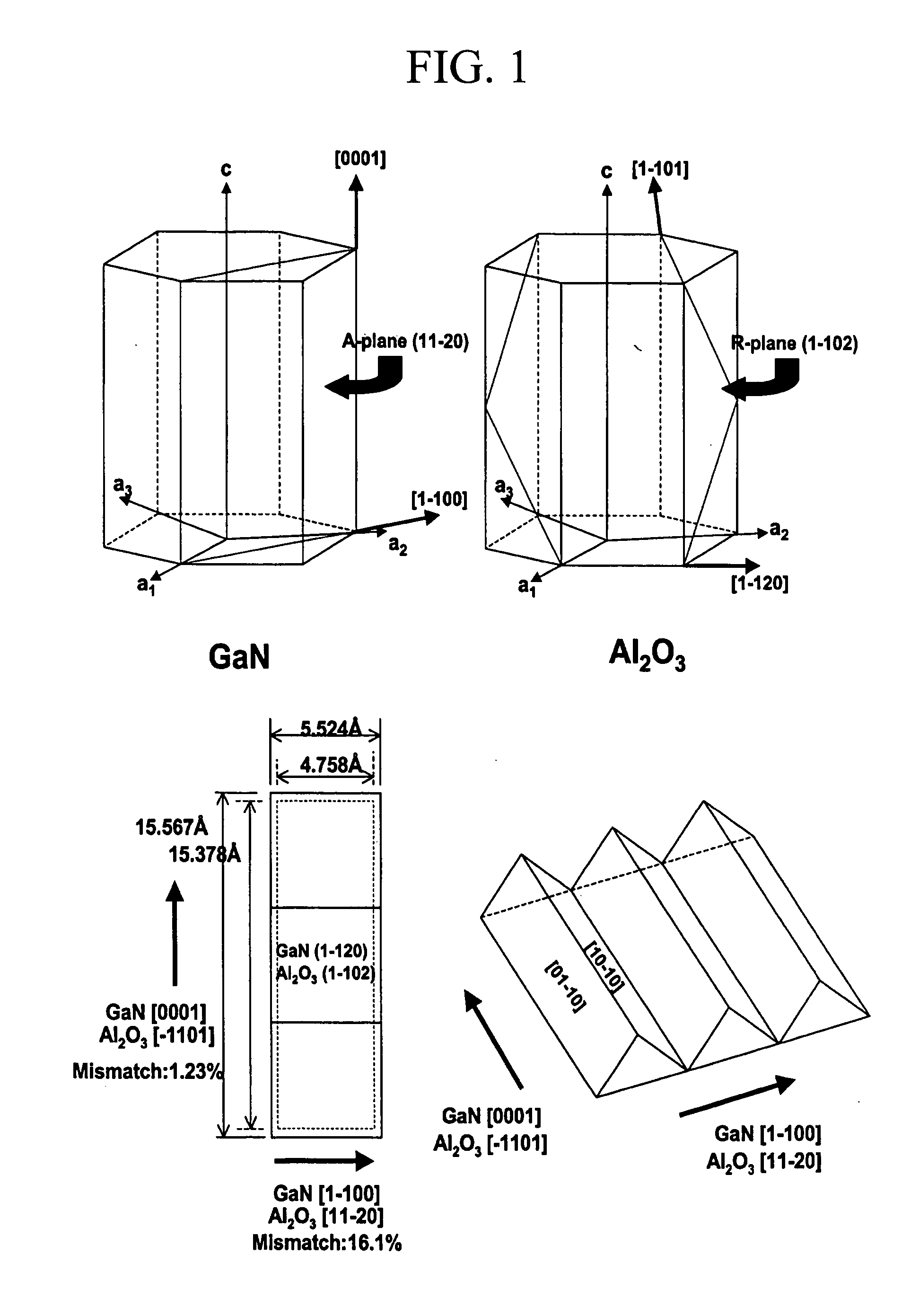
a technology of a-plane nitride and semiconductor wafers, which is applied in the direction of crystal growth process, polycrystalline material growth, coupling device connection, etc., can solve the problems of c-plane sapphire substrates that are not yet commercially available, c-plane nitride films grown on c-plane sapphire substrates tend to generate cracks, and achieve high quality

Inactive Publication Date: 2005-11-10
SAMSUNG CORNING CO LTD
View PDF5 Cites 134 Cited by
  • Summary
  • Abstract
  • Description
  • Claims
  • Application Information

AI Technical Summary

Benefits of technology

[0007] Accordingly, it is an object of the present invention to provide a high quality non-po

Problems solved by technology

Such c-plane nitride films grown on c-plane sapphire substrates, however, tend to generate cracks due to the differences in the lattice parameter and thermal expansion coefficient at the interface during a growth process.
This crack problem is more serious in case of c-plane nitride films doped with elements such as silicon.
Nevertheless, such a-plane nitride film substrates are not yet commercially available for the reason that when an a-plane nitride film i

Method used


Image

  • Non-polar single crystalline a-plane nitride semiconductor wafer and preparation thereof
  • Non-polar single crystalline a-plane nitride semiconductor wafer and preparation thereof
  • Non-polar single crystalline a-plane nitride semiconductor wafer and preparation thereof

Examples


example 1

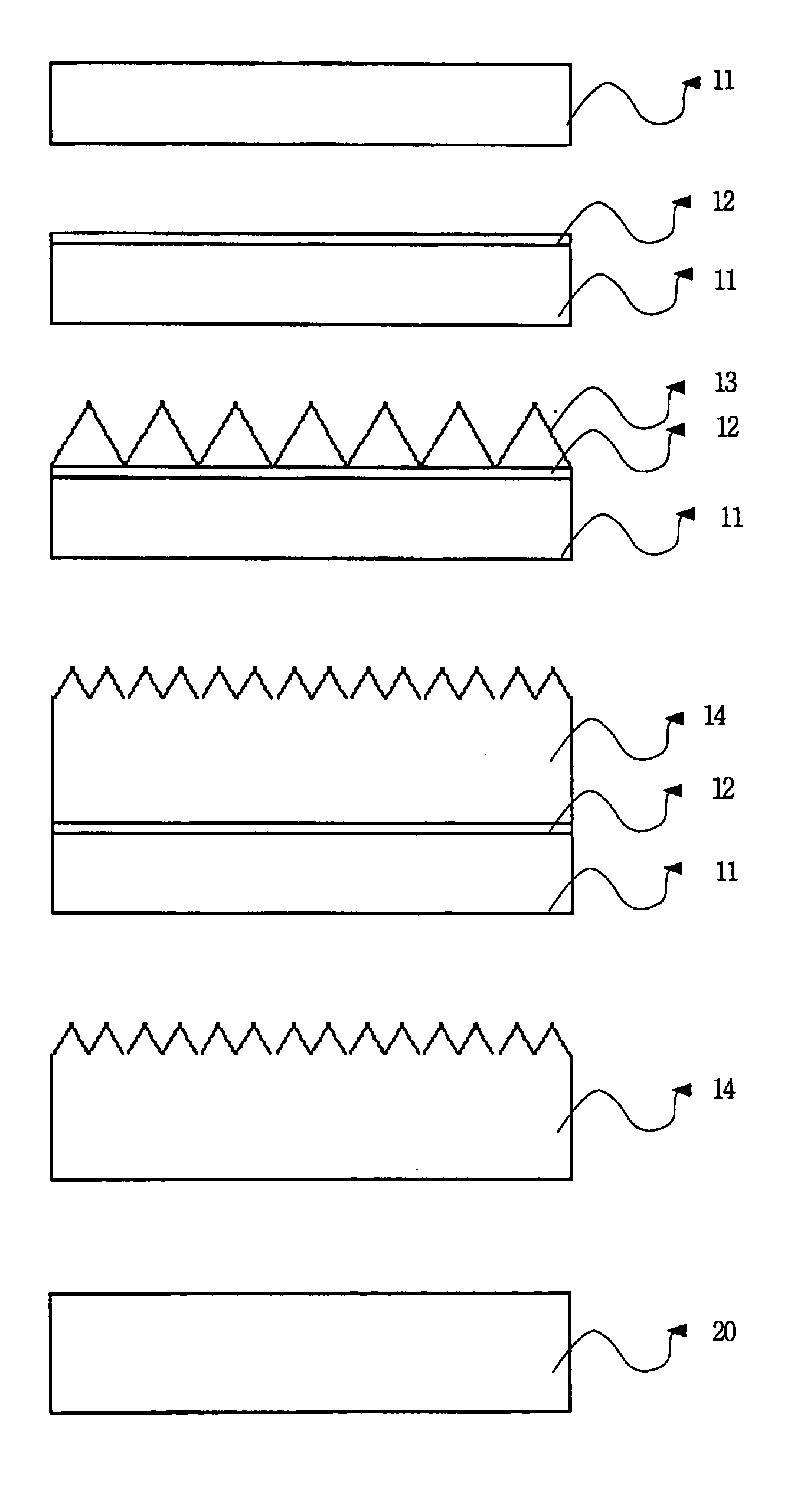
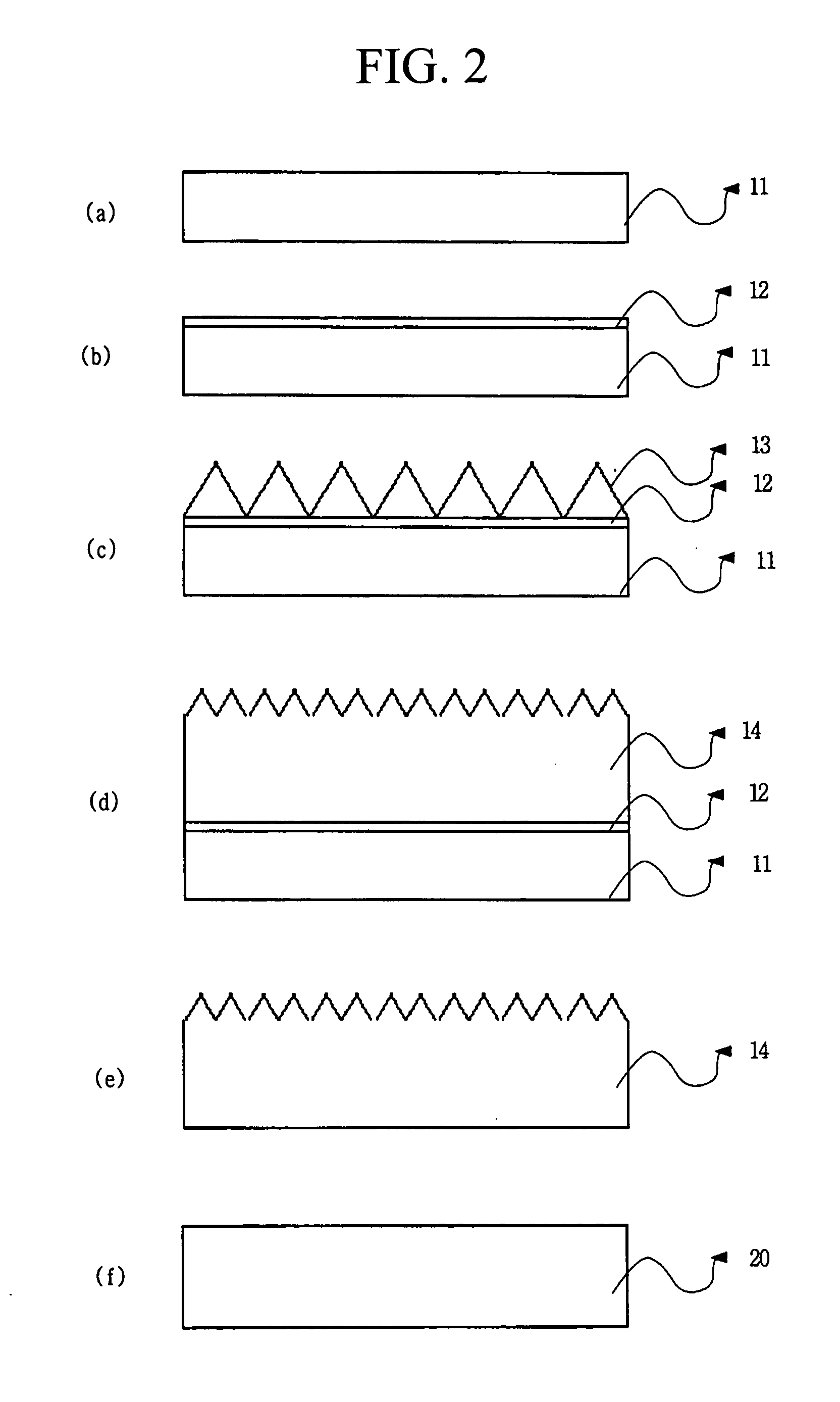
[0036] A single crystalline r-plane sapphire substrate with a 50.8 mm-diameter was loaded in an HVPE reactor, and nitridated at 950˜1,100° C. successively with gaseous ammonia, a gas mixture of ammonia and hydrogen chloride, and gaseous ammonia.

[0037] On the nitridated substrate thus obtained, a gallium nitride single crystal film was allowed to grow at a rate of 75 μm / hr by bringing gaseous gallium chloride and gaseous ammonia into contact therewith at 1,000° C. The gallium chloride gas, generated by reacting gallium with hydrogen chloride, and the gaseous ammonia were introduced through two separate inlets at a gaseous hydrogen chloride:ammonia volume ratio of 1:6. The reactor chamber was maintained at a temperature ranging from 600 to 900° C. under an ambient pressure. The growth of gallium nitride single crystal film was conducted for 400 minutes to form a 500 μm-thick gallium nitride semiconductor film on the substrate.

[0038] A photograph and an X-ray diffraction (XRD) patter...

example 2

[0041] The procedure of Example 1 was repeated except that the volume ratio of the gaseous hydrogen chloride and ammonia was in the range of 1:2˜5, to form a 500 μm-thick gallium nitride semiconductor film on the sapphire substrate.

[0042] An SEM photograph and an XRD rocking curve of the surface of the a-plane GaN thick film thus formed are shown in FIGS. 8A and 8B, respectively. The XRD rocking curve of FIG. 8B reveals that the a-plane nitride film possesses an FWHM value of 342 arcsec, the smallest among the hitherto-reported values, which indicates that the film crystallinity was significantly enhanced.

[0043] As described above, in accordance with the method of the present invention, a high quality non-polar single crystalline a-plane nitride semiconductor wafer having no voids, bending or cracks may be rapidly and effectively prepared and it may be advantageously used as a substrate in the manufacture of an LED.


PUM

PropertyMeasurementUnit
Temperatureaaaaaaaaaa
Thicknessaaaaaaaaaa
Thicknessaaaaaaaaaa

Abstract

A single crystalline a-plane nitride semiconductor wafer having no voids, bending or cracks can be rapidly and effectively prepared by hydride vapor phase epitaxy (HVPE) growth of the a-plane nitride semiconductor film on a single crystalline r-plane sapphire substrate at a temperature ranging from 950 to 1,100° C. and at a rate ranging from 30 to 300 μm/hr.

Description

FIELD OF THE INVENTION [0001] The present invention relates to a non-polar single crystalline a-plane nitride semiconductor wafer having no voids, bending or cracks, and a method for preparing said nitride semiconductor wafer. BACKGROUND OF THE INVENTION [0002] Single crystalline nitride-based wafers employed as substrates in manufacturing semiconductor devices are mostly c-plane ({0001}-plane) thin films which are grown on c-plane sapphire substrates by a conventional method, e.g., metal organic chemical vapor deposition (MOCVD), molecular beam epitaxy (MBE) and hydride vapor phase epitaxy (HVPE), and then separated therefrom. [0003] Such c-plane nitride films grown on c-plane sapphire substrates, however, tend to generate cracks due to the differences in the lattice parameter and thermal expansion coefficient at the interface during a growth process. This crack problem is more serious in case of c-plane nitride films doped with elements such as silicon. Also, the c-plane nitride f...

Claims


Application Information

Patent Timeline
IPC IPC(8): C23C16/34C30B29/38C30B25/02C30B25/18C30B29/40H01L21/205
CPCC30B25/02C30B29/403C30B25/18H01R13/4532
Inventor SHIN, HYUNMINLEE, HAE-YONGLEE, CHANGHOKIM, HYUN-SUKKIM, CHONG-DONKONG, SUN-HWAN
Owner SAMSUNG CORNING CO LTD
Why Eureka
Try Eureka