

Method and apparatus to increase throughput of processes using pulsed radiation sources
a technology of pulsed radiation and process, applied in metal working apparatus, manufacturing tools, welding/soldering/cutting articles, etc., can solve the problems of limited total throughput for exposing a material and limited total exposure time for the material
- Summary
- Abstract
- Description
- Claims
- Application Information
AI Technical Summary
Benefits of technology
Problems solved by technology
Method used
Image

Examples
Embodiment Construction
.
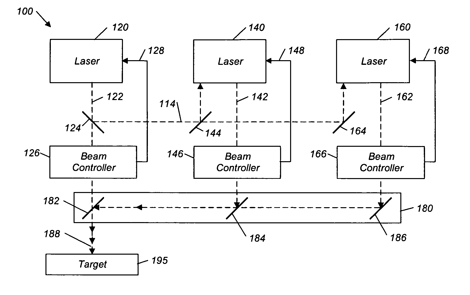
[0023] In the following description of exemplary embodiments of the present invention, a pulsed radiation source 120 may comprise an excimer laser. This excimer laser may be a laser light source such as, for example, KrF (248 nm wavelength), ArF (193 nm wavelength, and F2 (157 nm wavelength). Additionally, the present invention may be practiced with other pulsed radiation sources 120, such as, for example, harmonic generators using larger wavelength lasers in combination to produce a shorter wavelength beam, metal vapor lasers, diode pumped solid state lasers, and extreme ultraviolet beam generators such as X-rays. Signals referred to in this description may travel on and refer to a variety of embodiments, such as a single conductor, a serial communication bus, a parallel communication bus, and electromagnetic radiation such as a Radio Frequency (RF) signal.
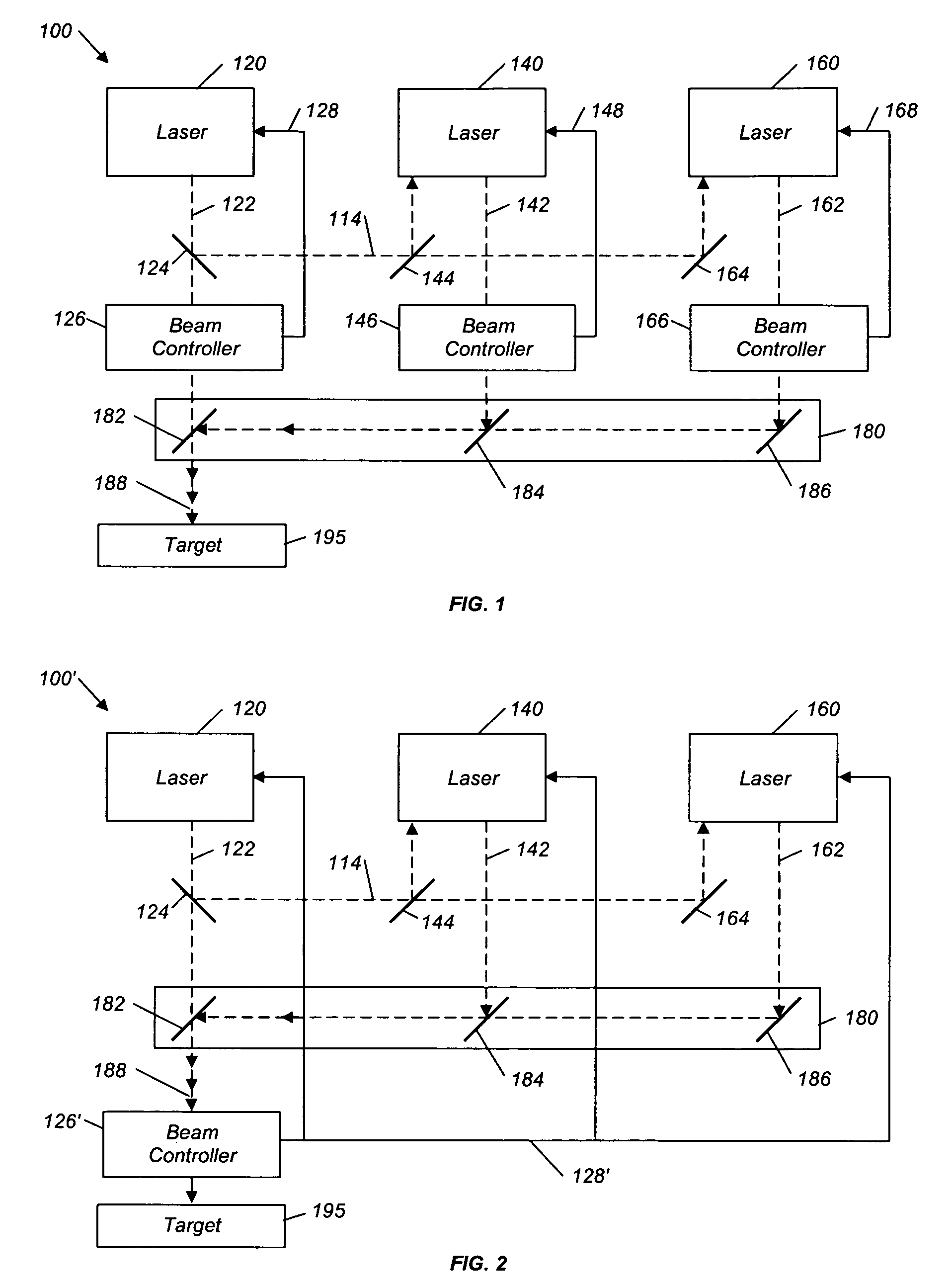
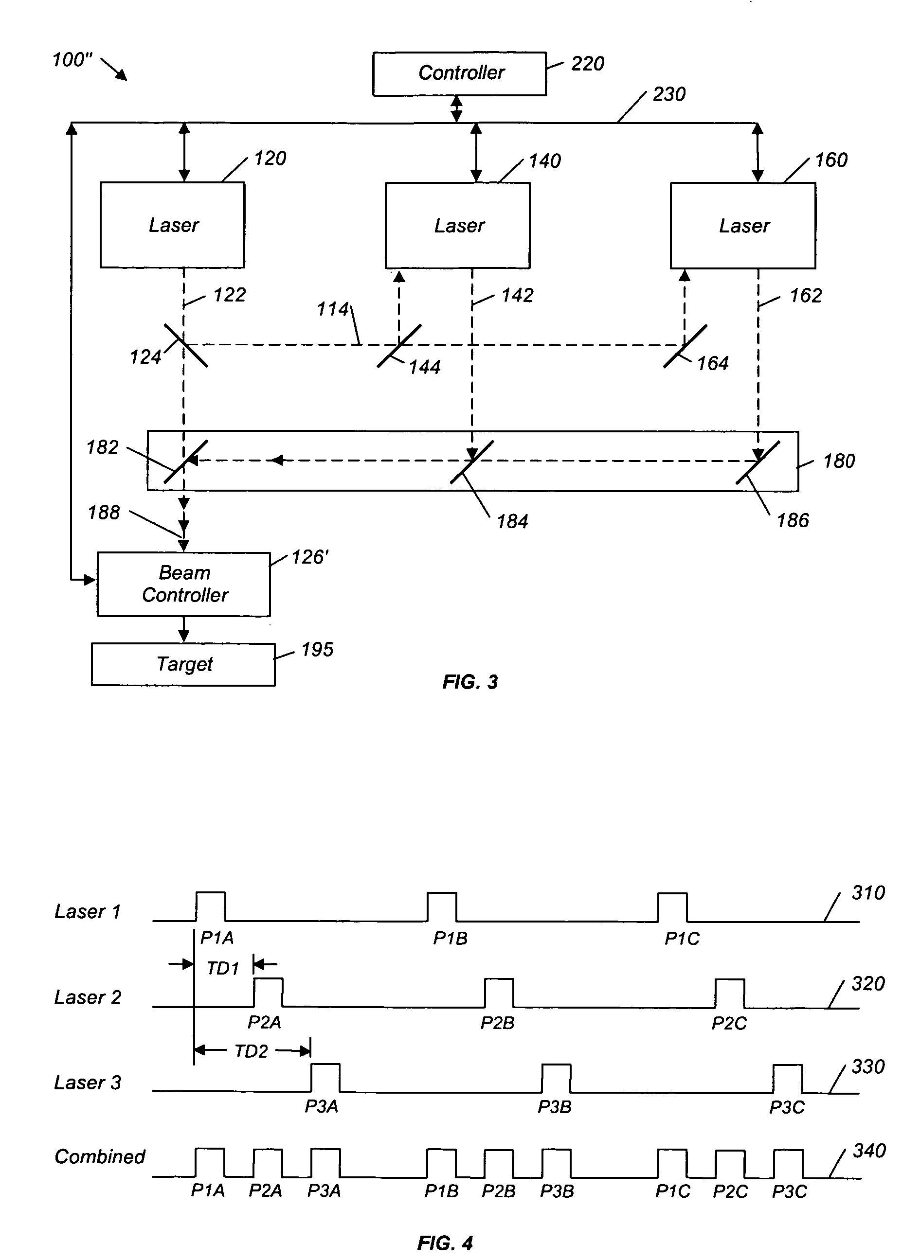
[0024]FIG. 1 illustrates an exemplary embodiment of the present invention. A pulsed radiation source 120 (also referred to as...
PUM
| Property | Measurement | Unit |
|---|---|---|
| Time | aaaaa | aaaaa |
| Wavelength | aaaaa | aaaaa |
| Pulsed sound | aaaaa | aaaaa |
Abstract
Description
Claims
Application Information