In situ doped epitaxial films

a doped epitaxial and film technology, applied in the direction of crystal growth process, polycrystalline material growth, chemically reactive gas, etc., can solve the problems of omitting photolithography and etch steps, reducing deposition rate, and slow deposition rate, so as to reduce deposition rate, slow deposition rate, the effect of slow deposition ra

Inactive Publication Date: 2005-11-10
ASM AMERICA INC
View PDF26 Cites 49 Cited by
  • Summary
  • Abstract
  • Description
  • Claims
  • Application Information

AI Technical Summary

Benefits of technology

[0005] Disadvantageously, many selective deposition chemistries tend to produce slow deposition rates, such that some or all of the throughput gained by omitting photolithography and etch steps is lost due to the slower deposition rate. Likewise, many in situ doping chemistries also have reduced deposition rates, such that some or all of the throughput gained by performing the doping in situ is lost due to the slower deposition rate. Especially problematic is high concentration n-type doping, such as doping with high concentrations of

Problems solved by technology

Disadvantageously, many selective deposition chemistries tend to produce slow deposition rates, such that some or all of the throughput gained by omitting photolithography and etch steps is lost due to the slower deposition rate.
Likewise, many in situ doping chemistries also have reduced deposition rates, such that some or all of the throughput gained by performing the doping in situ is lost due to the slower deposition rate.
Especially problemat

Method used


Image

  • In situ doped epitaxial films
  • In situ doped epitaxial films
  • In situ doped epitaxial films

Examples


Embodiment Construction

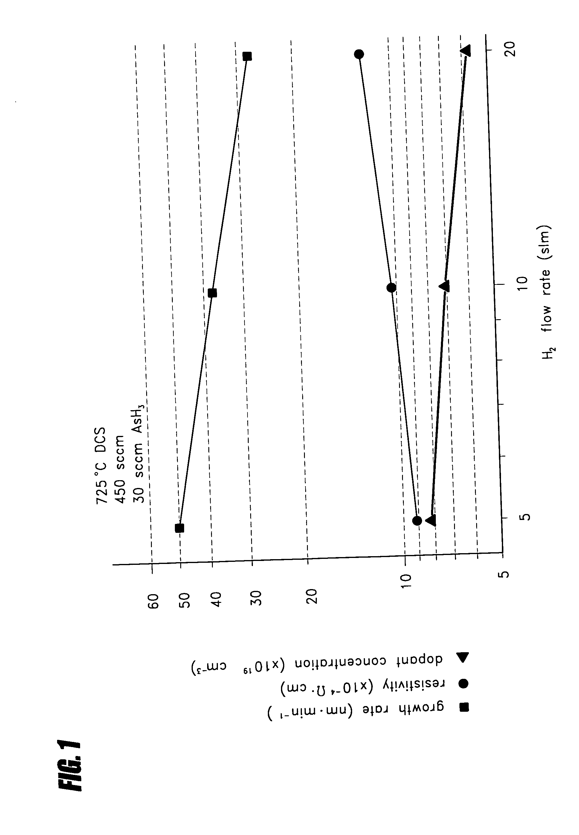
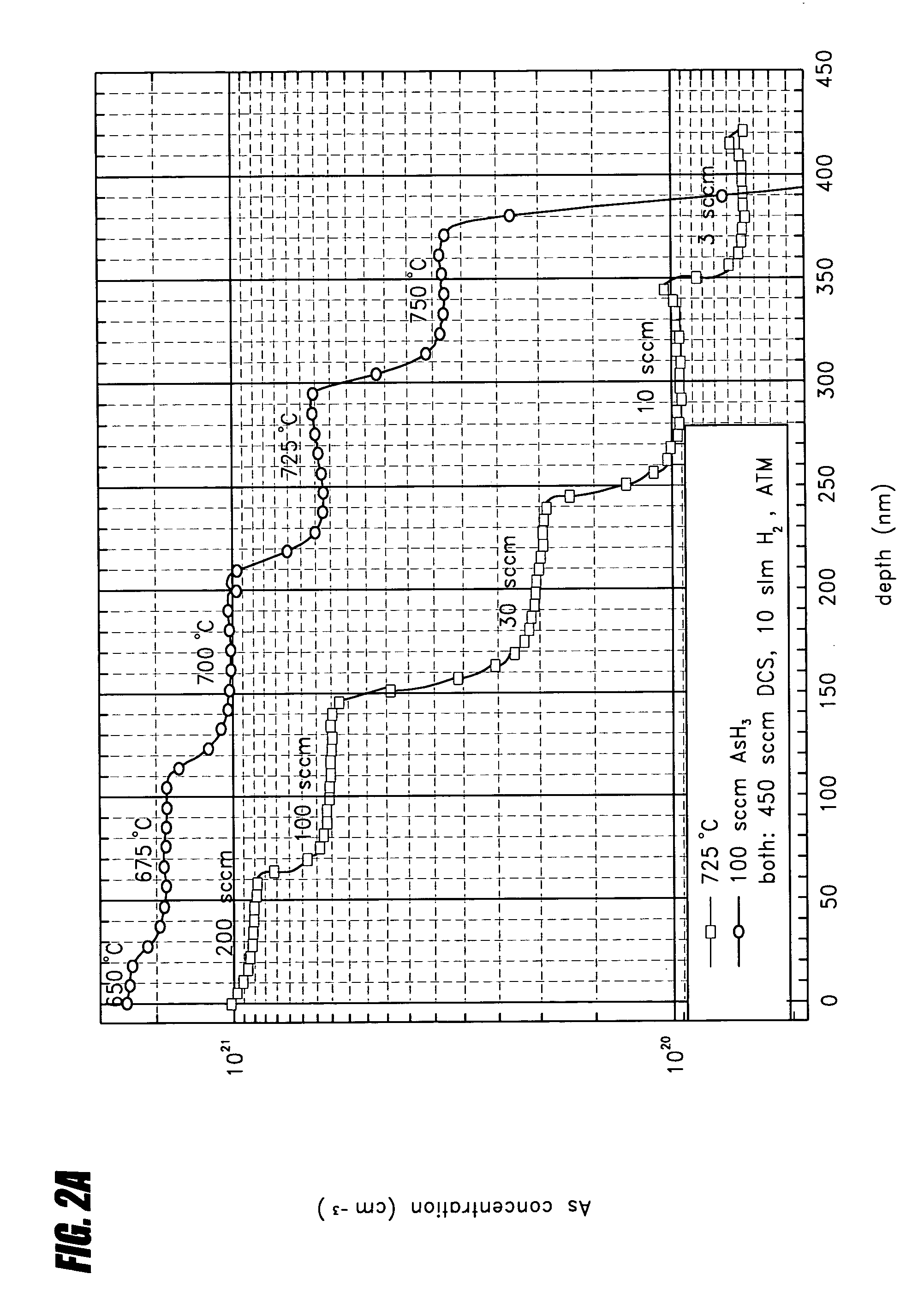
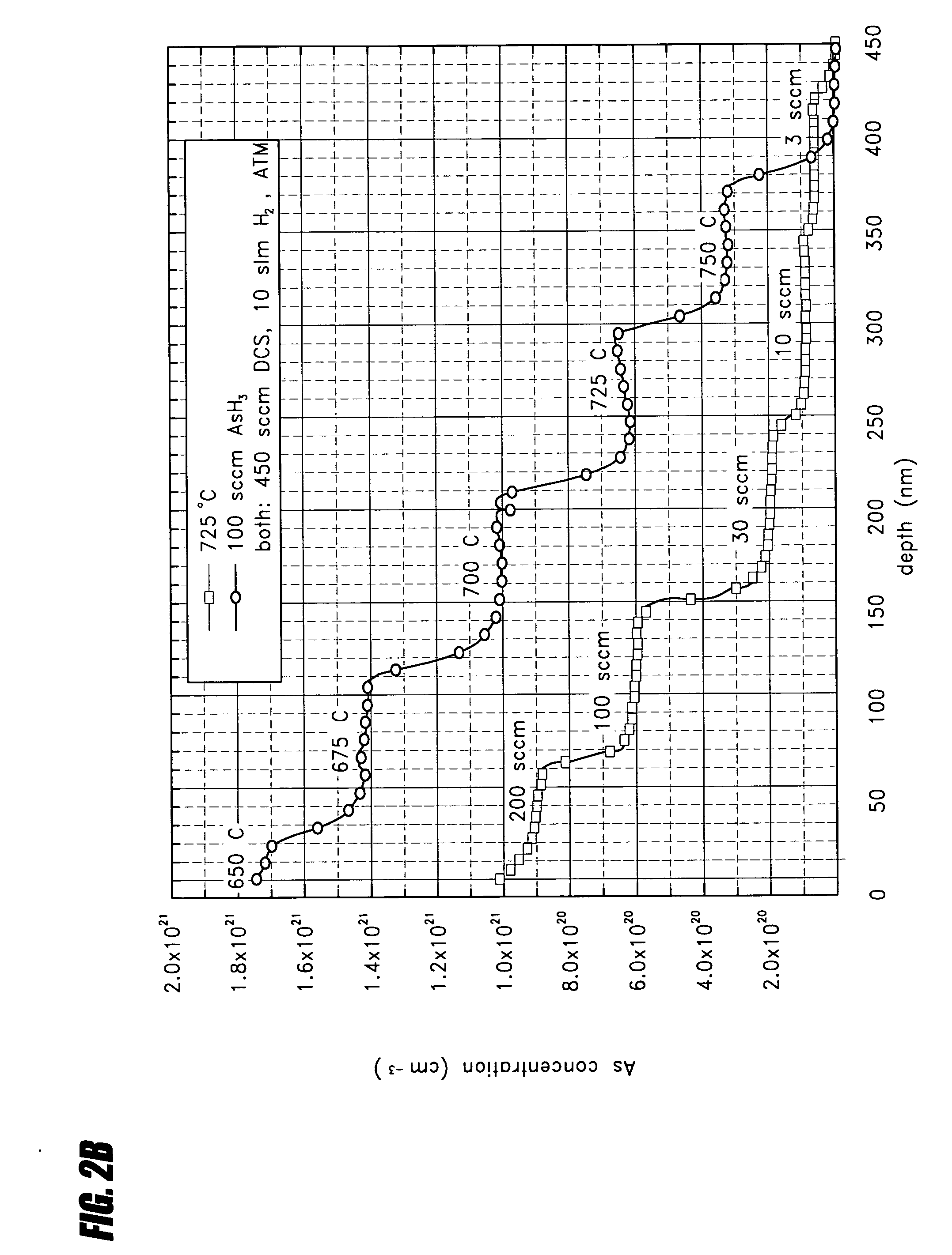
[0023] Disclosed herein are exemplary embodiments of improved methods for performing selective epitaxial deposition of semiconductor materials, including in situ doped semiconductor materials. Exemplary semiconductor materials that are deposited using certain of the embodiments disclosed herein include silicon films and silicon germanium films. Certain of the chemical vapor deposition (“CVD”) techniques disclosed herein produce semiconductor films with improved crystal quality, improved electrical activation of incorporated dopants, and increased growth rate. In certain embodiments, highly doped selective deposition is possible under atmospheric conditions using dichlorosilane (“DCS”) as a silicon precursor, dopant hydrides, and optionally, HCl to improve selectivity. Germanium and / or carbon precursors, such as germane or methylsilane, are optionally added to the process gas mixture to form films that include germanium and / or carbon.

[0024] Deposition at pressures above the LPCVD an...


PUM


Abstract

A method for depositing an in situ doped epitaxial semiconductor layer comprises maintaining a pressure of greater than about 80 torr in a process chamber housing a patterned substrate. The method further comprises providing a flow of dichlorosilane to the process chamber. The method further comprises providing a flow of a dopant hydride to the process chamber. The method further comprises selectively depositing the epitaxial semiconductor layer on single crystal material on the patterned substrate at a rate of greater than about 3 nm min−1.

Description

REFERENCE TO PRIORITY APPLICATIONS [0001] This application claims the benefit of U.S. Provisional Patent Application 60 / 565,033 (filed 23 Apr. 2004) and U.S. Provisional Patent Application 60 / 565,909 (filed 27 Apr. 2004). The entire disclosure of both of these priority applications is hereby incorporated by reference herein.FIELD OF THE INVENTION [0002] The present invention relates generally to selective epitaxial deposition, and more particularly to in situ rapid deposition of doped semiconductor layers. BACKGROUND OF THE INVENTION [0003] Improvement of wafer throughput is a continuing challenge in the semiconductor industry, especially with respect to single wafer processing. In single wafer processing, individual wafers are processed sequentially in a single processing tool. Improved wafer throughput generally leads to reduced costs and improved operating margins. [0004] One application in which increased wafer throughput is beneficial is in epitaxial deposition of semiconductor...

Claims


Application Information

Patent Timeline
IPC IPC(8): C30B1/00C30B25/02C30B25/16C30B29/52H01L21/20H01L21/205H01L21/285H01L21/31H01L21/36H01L21/469
CPCC30B25/02C30B25/16C30B29/52H01L21/02532H01L21/28562H01L21/02579H01L21/0262H01L21/02636H01L21/28525H01L21/02576H01L21/20
Inventor BAUER, MATTHIAS
Owner ASM AMERICA INC
Why Eureka
Try Eureka