Cvd apparatus having means for cleaning with fluorine gas and method of cleaning cvd apparatus with fluorine gas

a technology of cvd apparatus and fluorine gas, which is applied in the direction of perfluorocarbon/hydrofluorocarbon capture, sustainable manufacturing/processing, and final product manufacturing. it can solve the problems of disconnection or short-circuit of a semiconductor circuit, contamination, and inability to manufacture high quality, etc., to achieve excellent cleaning uniformity, excellent etching speed, and easy to obtain

Inactive Publication Date: 2005-11-17
NAT INST OF ADVANCED IND SCI & TECH +12
View PDF7 Cites 26 Cited by
  • Summary
  • Abstract
  • Description
  • Claims
  • Application Information

AI Technical Summary

Benefits of technology

[0037] Thus, the energy is simply applied to react the fluorine compound so that the fluorine gas component and the component other than the fluorine gas component are generated and separated. Consequently, the fluorine gas component is separated and refined so that the fluorine gas can easily be obtained.
[0038] Accordingly, after the film forming process for the base material is carried out by the CVD apparatus, the fluorine gas thus obtained is then converted to a plasma. By using the plasma to remove a by-product adhered into the reaction chamber, it is possible to obtain a very excellent etching speed. Thus, an excellent cleaning uniformity can be maintained.
[0039] In addition, such a fluorine gas generating device has a smaller size as compared with a conventional fluorine gas generating device using electrolysis, and furthermore, the fluorine gas can be obtained efficiently. The CVD apparatus itself is also small-sized and maintenance can easily be carried out.

Problems solved by technology

At the film forming step, consequently, fine particles to be foreign matters are mixed into the semiconductor product so that contamination is caused.
For this reason, a thin film of high quality cannot be manufactured so that the disconnection or short-circuit of a semiconductor circuit is caused.
In addition, there is a possibility that a yield or the like might be deteriorated.
Furthermore, there is a problem in that a gas discharging process is hard to perform after the cleaning and a disposal cost is increased.
Therefore, it has an adverse influence on global warming, and a dissociation efficiency is low and a cleaning capability is also low.
If the concentration of the cleaning gas is more than a certain concentration, however, there is a problem in that the generation of a plasma becomes unstable, the etching speed is decreased or a cleaning uniformity is deteriorated.
If the cleaning gas is used in a concentration of 100%, particularly, there is a problem in that the instability of the generation of the plasma, the decrease in the etching speed and the deterioration in the cleaning uniformity tend to be more remarkable so that a utility cannot be obtained.
If the chamber pressure is raised or the gas flow is increased in the cleaning, however, the generation of a plasma becomes unstable and the cleaning uniformity is deteriorated so that the cleaning cannot be efficiently carried out.
Such a conventional fluorine gas generating device is large-sized and cannot be used safely.
If the fluorine gas generating device is used in a CVD apparatus, the size of the CVD apparatus is increased, and furthermore, a complicated work is required for maintenance and control.
Also when a fluorine gas cylinder is provided in the CVD apparatus in place of the conventional fluorine gas generating device, accordingly, the size of the apparatus is increased, and furthermore, the exchange of the cylinder is complicated, which is inconvenient.

Method used


Image

  • Cvd apparatus having means for cleaning with fluorine gas and method of cleaning cvd apparatus with fluorine gas
  • Cvd apparatus having means for cleaning with fluorine gas and method of cleaning cvd apparatus with fluorine gas
  • Cvd apparatus having means for cleaning with fluorine gas and method of cleaning cvd apparatus with fluorine gas

Examples


example 1

[0119] Cleaning using a Fluorine Compound (FNO) Containing Nitrogen

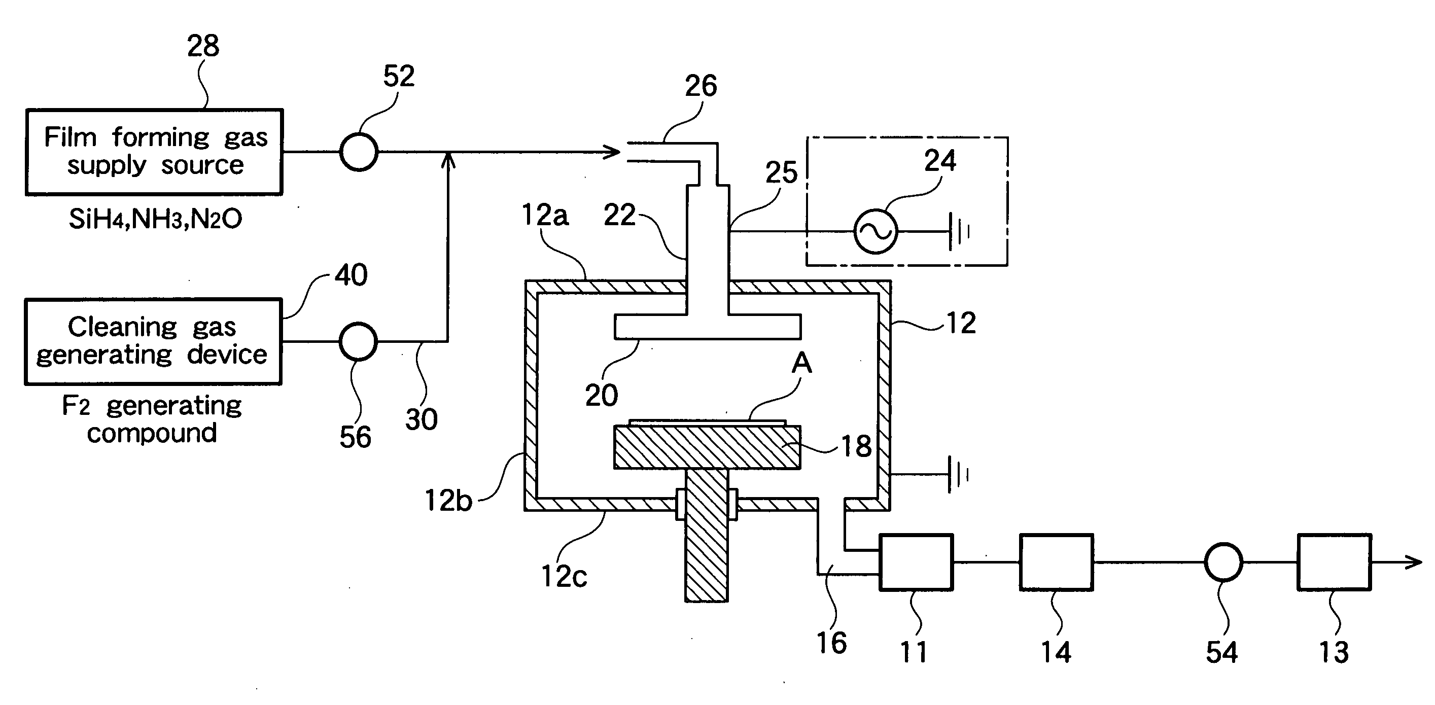
[0120] As shown in FIG. 1, a silicon wafer was mounted on the stage of the lower electrode 18 of the reaction chamber 12 and monosilane (SiH4) and N2O were supplied in a ratio of 70:2000 as a film forming gas from the film forming gas supply source 28. The inside of the reaction chamber 12 was maintained in a decompression state of 200 Pa and a high frequency electric field of 13.56 Hz was generated from the high frequency applying device 25 over the upper electrode 20. As a result, a high frequency plasma was formed so that a thin SiO2 film was formed on the surface of the base material A of the silicon wafer.

[0121] In this case, a by-product such as SiO2 was adhered to and deposited on the surfaces of an internal wall, an electrode and the like in the reaction chamber 12.

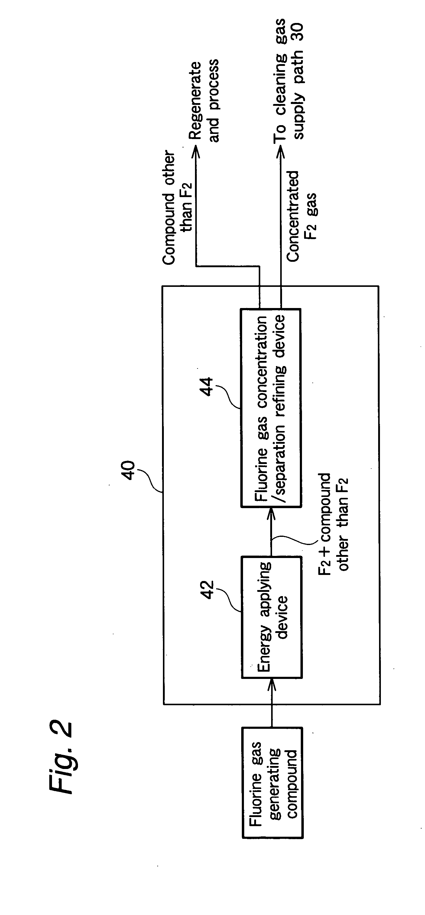
[0122] In the cleaning gas generating device 40, then, FNO was used as a cleaning gas material comprising a fluorine compound and was diluted w...

example 2

[0126] Cleaning using a Fluorine Compound (ClF3) Containing Chlorine

[0127] As shown in FIG. 5, a thin SiO2 film was formed on the surface of the base material A of a silicon wafer in the same manner as in the example 1. In this case, a by-product such as SiO2 was adhered to and deposited on the surfaces of an internal wall, an electrode and the like in the reaction chamber 12.

[0128] In the cleaning gas generating device 40, then, ClF3 was used as a cleaning gas material comprising a fluorine compound, and a heating device was used as the energy applying device 42. As a result, the ClF3 was thermally decomposed at an atmospheric pressure and a temperature of 450° C. through heating in an electric furnace, so that ClF and F2 were generated.

[0129] Then, the ClF and the F2 thus generated were separated into the ClF and the F2 by using a distilling device as the fluorine gas concentration / separation refining device 44 and liquid nitrogen as a refrigerant.

[0130] The F2 thus separated ...

example 3

[0132] Cleaning using a Fluorine Compound (COF2) Containing Carbon

[0133] As shown in FIG. 6, SiH4, NH3 and N2 were supplied in a ratio of 180:320:1000 to form a thin SiN film on the surface of the base material A of a silicon wafer in the same manner as in the example 1. In this case, a by-product such as Si3N4 was adhered to and deposited on the surfaces of an internal wall, an electrode and the like in the reaction chamber 12.

[0134] In the cleaning gas generating device 40, then, COF2 was used as a cleaning gas material comprising a fluorine compound and was supplied to the energy applying device 42 in a mole ratio of COF2 / O2=9. A plasma generating device was used as the energy applying device 42 and decomposition was carried out at 13.56 MHz and 200 Pa to generate CO, CO2, F2 or the like.

[0135] The gas thus generated was pressurized to have an atmospheric pressure. By utilizing a liquid trapping device as the fluorine gas concentration / separation refining device 44, then, rema...


PUM

PropertyMeasurementUnit
frequencyaaaaaaaaaa
pressureaaaaaaaaaa
boiling pointaaaaaaaaaa

Abstract

It is an object to provide a cleaning method in a CVD apparatus capable of efficiently removing a by-product such as SiO2 or Si3N4 which is adhered to and deposited on the surfaces of an inner wall, an electrode and the like in a reaction chamber at a film forming step. Furthermore, it is an object to provide a cleaning method in which the amount of a cleaning gas to be discharged is very small, an influence on an environment such as global warming is also lessened and a cost can also be reduced. An energy is applied to a fluorine compound to react the fluorine compound, thereby generating a fluorine gas component and a component other than the fluorine gas component. Furthermore, the fluorine gas component and the component other than the fluorine gas component which are generated are separated from each other so that the fluorine gas component is separated and refined. After a film forming process for a base material is carried out by a CVD apparatus, a separated and refined fluorine gas is then converted to a plasma to remove a by-product adhered into the reaction chamber.

Description

TECHNICAL FIELD [0001] The present invention relates to a chemical vapor deposition (CVD) apparatus for forming a uniform thin film of high quality, for example, silicon oxide (SiO2) or silicon nitride (Si3N4 or the like) on a surface of a base material for a semiconductor such as a silicon wafer. [0002] In more detail, the present invention relates to a CVD apparatus capable of executing cleaning for removing a by-product adhered to an inner wall of a reaction chamber or the like after a thin film forming process, and a method of cleaning the CVD apparatus using the same. BACKGROUND ART [0003] Conventionally, a thin film such as silicon oxide (SiO2) or silicon nitride (Si3N4 or the like) is widely used in a semiconductor element such as a thin film transistor, a photoelectric converting element or the like. The following three kinds of techniques for forming a thin film such as silicon oxide, silicon nitride or the like are mainly used. [0004] (1) Physical vapor-phase film forming ...

Claims


Application Information

Patent Timeline
Patent Type & Authority Applications(United States)
IPC IPC(8): B08B7/00C23C16/44H01J37/32H01L21/3065H01L21/31
CPCB08B7/0035C23C16/4405Y02C20/30H01J37/32862H01J37/32357Y02P70/50H01L21/205
Inventor BEPPU, TATSUROSAKAI, KATSUOOKURA, SEIJISAKAMURA, MASAJIABE, KAORUMURATA, HITOSHIWANI, ETSUOKAMEDA, KENJIMITSUI, YUKIOHIRA, YUTAKAYONEMURA, TAISUKESEKIYA, AKIRA
Owner NAT INST OF ADVANCED IND SCI & TECH
Why Eureka
Try Eureka