Circuit board and semiconductor device using the same

a technology of circuit board and semiconductor device, which is applied in the direction of printed circuit, printed circuit stress/warp reduction, conductive pattern reinforcement, etc., can solve the problems of easy deterioration of reliability, large area of circuit board and brazing portion, and breakdown of ceramic insulated board having brittle properties in mechanical structure, etc., to achieve excellent heat radiation property, reduce thermal stress or thermal strain, and low cost

Inactive Publication Date: 2005-11-24
HITACHI METALS LTD
View PDF0 Cites 18 Cited by
  • Summary
  • Abstract
  • Description
  • Claims
  • Application Information

AI Technical Summary

Benefits of technology

[0024] An object of the present invention is to provide a highly reliable and low cost semiconductor device which can alleviate thermal stress or thermal strain generated during manufacture and operation and can also eliminate possibility in deformation, denaturation, and breakdown of each member.
[0027] The structure described above can maintain the excellent heat radiation property and reliability and moreover is capable of making contribution to acquisition of a low cost semiconductor device. The ceramics board described above is also characterized in that it is formed of at least a kind of material selected from a group of silicon nitride, aluminum nitride, and alumina.
[0029] As described above, the present invention can provide a low cost semiconductor device which can alleviate thermal stress or thermal strain which is generated during manufacture or operation, provides least possibility of deformation, denaturation, and breakdown of each member, and assures excellent heat radiation property and higher reliability.
[0030] In more practical, a thermal resistance of 0.4° C. / W or less can be attained and excellent flatness with less curvature can be acquired to realize electrically stable operation by selecting copper or copper alloy for the wiring metal board and using a copper system material having the thermal expansion coefficient smaller than that of the wiring metal board for the metal board in the heat radiating side. Here, the reason why the copper system material is used for the metal board in the heat radiating side is that the copper element plastically deforms during the cooling process of the bonding process and such deformation will provide the effect to reduce a residual stress applied to the ceramics board in the bonding process.
[0031] Moreover, since the number of bonding areas is reduced, long-term reliability can be attained easily and the manufacturing process can also be simplified. Therefore, remarkable cost reduction may also be realized. As the ceramics board mounted on a circuit board, it is also possible to apply aluminum nitride and alumina, in addition to silicon nitride. A plurality of ceramics board may also be mounted as required. In this case, it is also possible to combine as required the silicon nitride board, aluminum nitride board and alumina board. However, when it is requested to further lower a thermal resistance using a thick circuit wiring board made of copper, alumina board or aluminum nitride board is insufficient in the strength and the silicon nitride board is most preferable.

Problems solved by technology

In this case, since difference in the thermal expansion coefficient between the cupper supporting member and the copper clad AlN board is large, reliability is easily deteriorated because of fracture of solder layer, shutdown of heat flowing path, and destruction of circuit board, etc.
Therefore, the area of circuit board and brazing portion becomes large.
Thermal stress during operation is repeated applied to the semiconductor device and if this thermal stress is superimposed to the residual thermal stress or thermal strain, the heat flowing path is shut down due to fatigue fracture of the solder layer (#2 solder layer described later, particularly) and breakdown occurs in the ceramics insulated board having brittle property in the mechanical structure.
Such event not only impedes the normal operation of a semiconductor device but also results in a problem in safety particularly represented by breakdown of the circuit board.
If curvature is generated in a semiconductor device, it is difficult to uniformly supply a thermal conductive grease at the time of mounting a semiconductor device to a cooling fin.
As a result, successful thermal engagement cannot be attained between the copper supporting member and the cooling fin and thereby heat radiating characteristic of this path is deteriorated, making it difficult to normally operate the semiconductor device.
Moreover, when the semiconductor device is mounted on the cooling fin through the screwing, a new external force is applied thereto, easily generating damage of circuit board.
(3) Problem in the Number of Assembling Processes and Difficulty in Lead-Free Soldering
However, it is difficult to obtain sufficient temperature hierarchical property from combination of the existing lead-free solder materials.
However, a problem of the item (3) is still left unsolved for the assembling of the semiconductor device because both processes to form the #1 solder and #2 solder layer are still necessary.
Moreover, a problem that cost becomes higher is still left because the alumina insulating member and the Al / SiC supporting member are manufactured with different processes.
In these processes, much cost is required and it finally impedes reduction in cost of the semiconductor device.
Moreover, the Al clad AlN board manufactured previously and an oxide substance formed on the surface of the Al / SiC heat sink are left at the interface after the junction, and therefore connection property and reliability of this interface is easily damaged.
However, in the case of this structure, since the Al / SiC base board and ceramics circuit board are integrated in direct under a comparatively higher temperature, stress, strain, and deformation by curvature are easily generated in the integrated boards, resulting in the problem described in the items (1) and (2).
The patent documents and non-patent document described above do not yet disclose solutions of such problems and the optimum structure for avoiding failures particularly in the manufacturing and operating condition of the semiconductor device.

Method used


Image

  • Circuit board and semiconductor device using the same
  • Circuit board and semiconductor device using the same
  • Circuit board and semiconductor device using the same

Examples


first embodiment

[0047] A semiconductor device as an embodiment of the present invention will be described below. First, the semiconductor device as the present invention will be described with reference to the accompanying drawings.

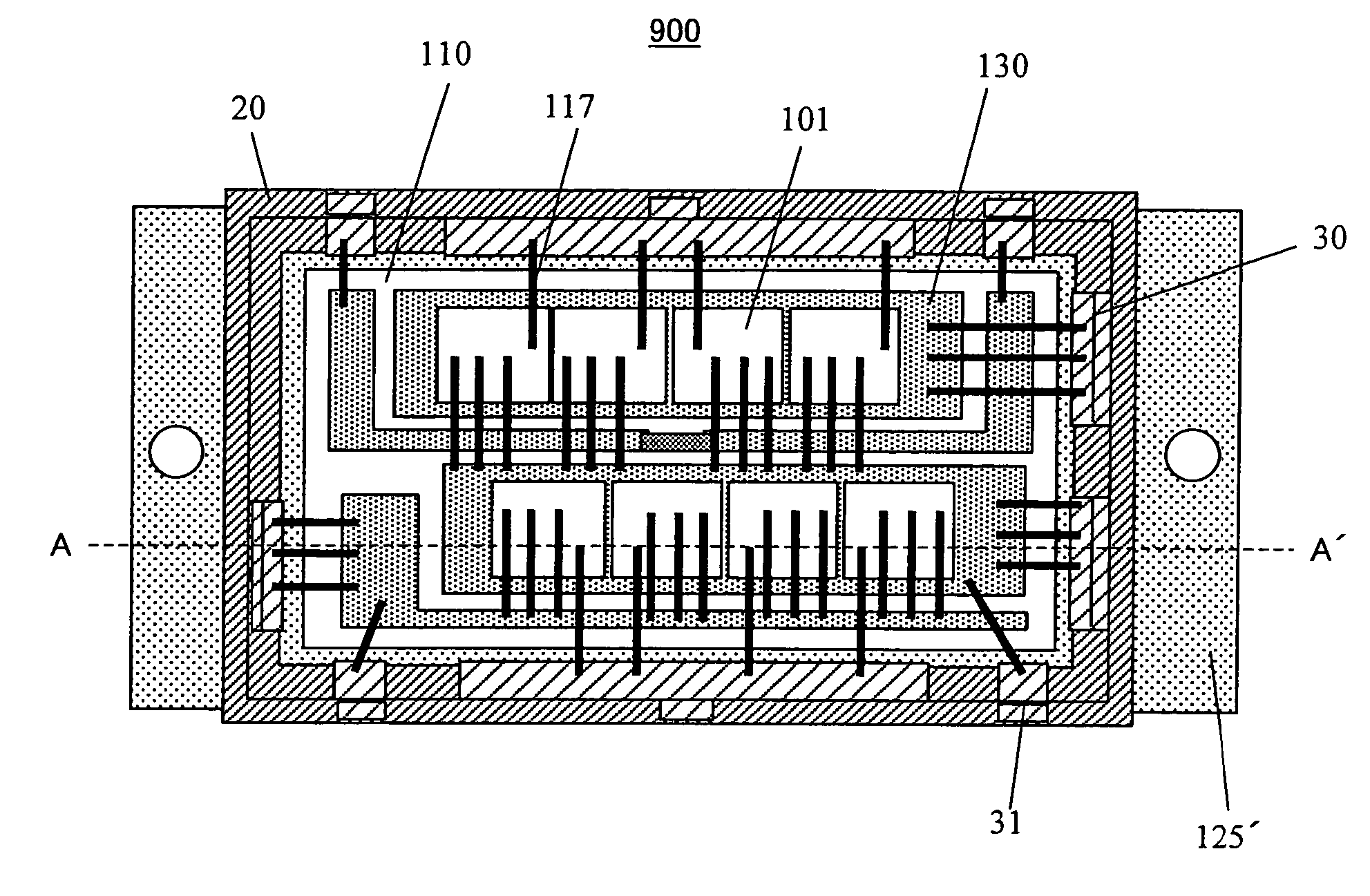
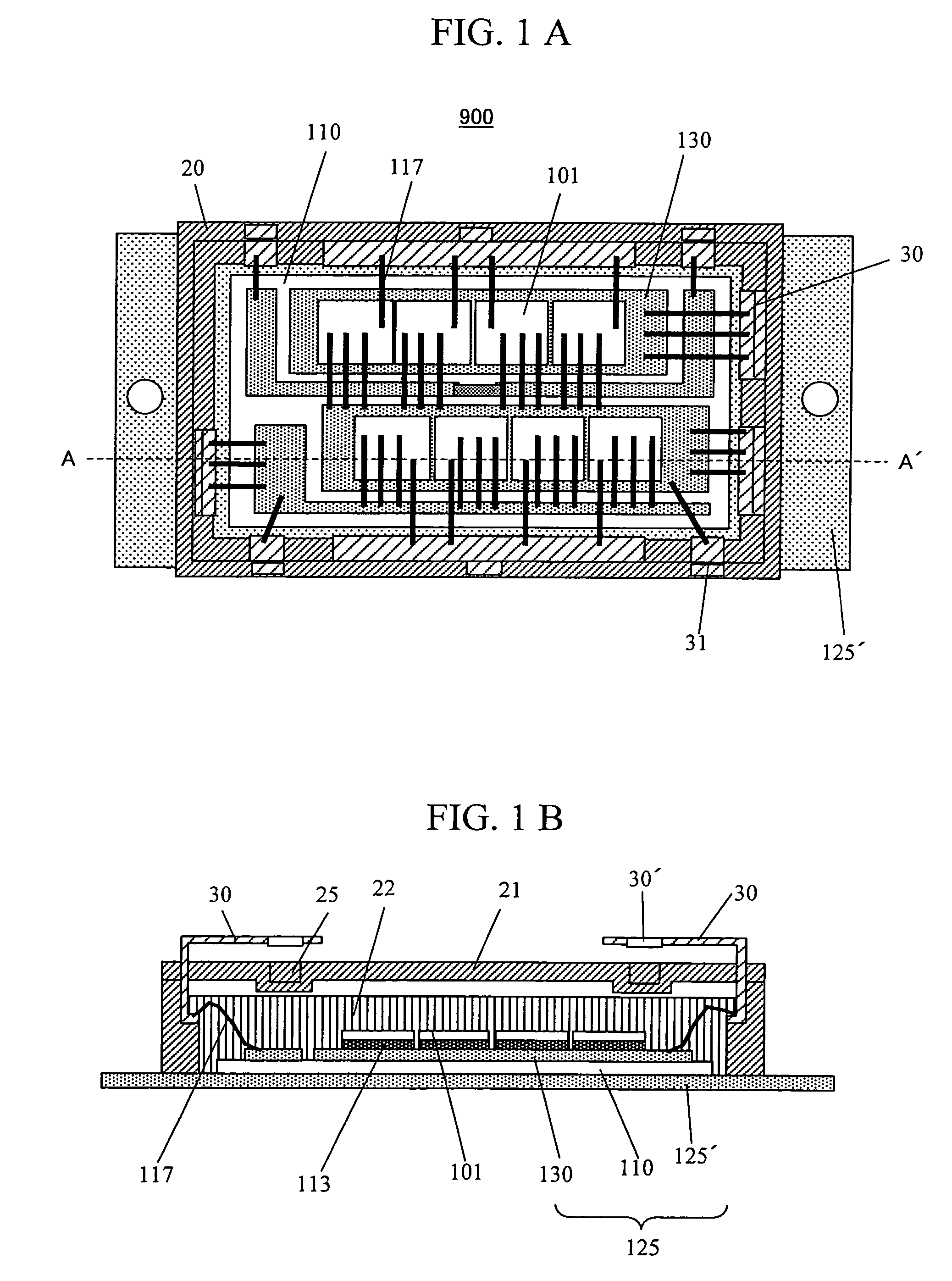
[0048]FIG. 1A and FIG. 1B illustrate examples of a basic structure of a semiconductor device as an embodiment of the present invention. FIG. 1A is a plan view of the semiconductor device, while FIG. 1B is a cross-sectional view along the line A-A′ in FIG. 1A. As illustrated in FIG. 1A and FIG. 1B, a semiconductor device 900 in this embodiment has a structure that a MOSFET element base material 101 is mounted as a semiconductor base material on a silicon nitride board 110 as a ceramics insulating board and a copper wiring board 130 provided on the silicon nitride board 110. Moreover, a polyphenyl sulphide resin case 20 provided with a main terminal 30 and an auxiliary terminal 31 is mounted to an insulated board (circuit board) 125.

[0049] In this embodiment, the insulate...

fourth embodiment

[0086]FIGS. 11A, 11B, and 11C are respectively a plan view of the front surface, a cross-sectional view and a plan view of the rear surface illustrating in detail an example of the structure of the composite metal board 125 used in the semiconductor device of this FIGS. 14A to 14D illustrate the principal manufacturing processes of the insulated semiconductor device of this embodiment. First, the manufacturing processes of the insulated board 125 will be described with reference to FIGS. 14A to 14D. A ceramics board is prepared first (FIG. 14A). After the Ag—Cu—Ti system brazing material paste is printed on the surface (front surface) of the ceramics board 110, a metal board (Cu board) for wiring is laminated on the front surface of the ceramics board 110, and the metal board 130a and ceramics board 110 are brazed (braze is designated as reference numeral 120b) through the heat treatment of the laminated body (FIG. 14B). Thereafter, the metal board 130a is etched preferably for sim...

sixth embodiment

[0096] Next, the present invention will be described with reference to the accompanying drawings. This embodiment may be adapted in common to all embodiments described above. FIGS. 12A and 12B schematically illustrate the insulated semiconductor device manufactured using the insulated board of this embodiment, while FIGS. 12C and 12D are schematically illustrate the insulated semiconductor device using an ordinary insulated board. FIGS. 12A and 12B are corresponding to each other. This embodiment will be described through comparison of these devices with reference to FIG. 12A to 12D.


PUM

PropertyMeasurementUnit
thicknessaaaaaaaaaa
thicknessaaaaaaaaaa
thicknessaaaaaaaaaa

Abstract

There is provided a thinner high frequency power module structure having reduced the mounting area. An insulated board is provided with a composite metal board in which the Cu2O powder particles are dispersed into a matrix metal (Cu) (amount of addition of Cu2O: 20 vol %; thermal expansion coefficient: 10.0 ppm / ° C.; thermal conductivity: 280 W / m•K; thickness: 1 mm; size: 42.4×85 mm), a silicon nitride board (thermal expansion coefficient: 3.4 ppm / ° C.; thermal conductivity: 90 W / m•K; thickness: 0.3 mm; size: 30×50 mm) deposited with Ag-system bonding metal layer to one principal surface of the composite metal board, and a wiring metal board formed of copper or copper alloy provided to the other principal surface of the ceramics insulated board. For example, the bonding metal layer is adjusted in the thickness to 50 μm, while the wiring metal board is also adjusted in the thickness to 0.4 mm. In the integrated board of the wiring and heat radiating boards, the Ni plating layer (thickness: 6 μm, not illustrated) is formed with the non-electrolyte wet plating process to the surface metal layer of the wiring metal board and composite metal board. This Ni plating layer is formed to the wiring metal boards in order to attain the solder bondability to mount the semiconductor base material with the brazing method and to enhance the wire bondability of the wiring metal board. Moreover, this Ni plating layer effectively prevents denaturation of the internal side by shutting off from the external atmosphere.

Description

[0001] This application is based on the Japanese Patent application No. 2004-148002, filed on May 18th, 2004, all the contents of which is incorporated in this application by reference. FIELD OF THE INVENTION [0002] The present invention relates to an insulated semiconductor device and particularly to an insulated semiconductor device in the structure using an insulating member as a bottom cover of a case. BACKGROUND OF THE INVENTION [0003] A semiconductor device having the structure in which a semiconductor element base material is mounted on a metal supporting member has a merit that a degree of freedom for application into a circuit is high because all electrodes can be guided to the external side under the condition electrically insulated from all package members including the metal supporting member. In the example of structure where a pair of main electrodes is floated from the ground potential, for example, mounting of a semiconductor device can be done easily because a packa...

Claims


Application Information

Patent Timeline
Patent Type & Authority Applications(United States)
IPC IPC(8): H01L23/12H01L21/48H01L23/14H01L23/373H01L23/52H05K1/02H05K1/03H05K1/05H05K3/24
CPCH01L21/4871H01L2924/10253H01L2224/48091H01L2224/49175H01L2224/73265H01L2924/01046H01L2924/01078H01L2924/01079H01L2924/19107H05K1/0271H05K1/0306H05K1/05H05K3/0061H05K3/244H05K2201/0209H05K2201/0355H05K2201/068H01L23/3735H01L2924/1301H01L24/48H01L24/49H01L2924/01019H01L2924/13091H01L2224/48227H01L2224/49111H01L2924/13055H01L2924/12041H01L2924/00014H01L2924/00H01L2924/181H01L2224/45124H01L24/45H01L2924/00012H01L2224/45015H01L2924/207
Inventor MORITA, TOSHIAKISUZUKI, KAZUHIROIMAMURA, HISAYUKIWATANABE, JUNICHICHIBA, MITSUAKI
Owner HITACHI METALS LTD
Why Eureka
Try Eureka