Methods of fabricating complex blade geometries from silicon wafers and strengthening blade geometries
- Summary
- Abstract
- Description
- Claims
- Application Information
AI Technical Summary
Benefits of technology
Problems solved by technology
Method used
Image
Examples
first embodiment
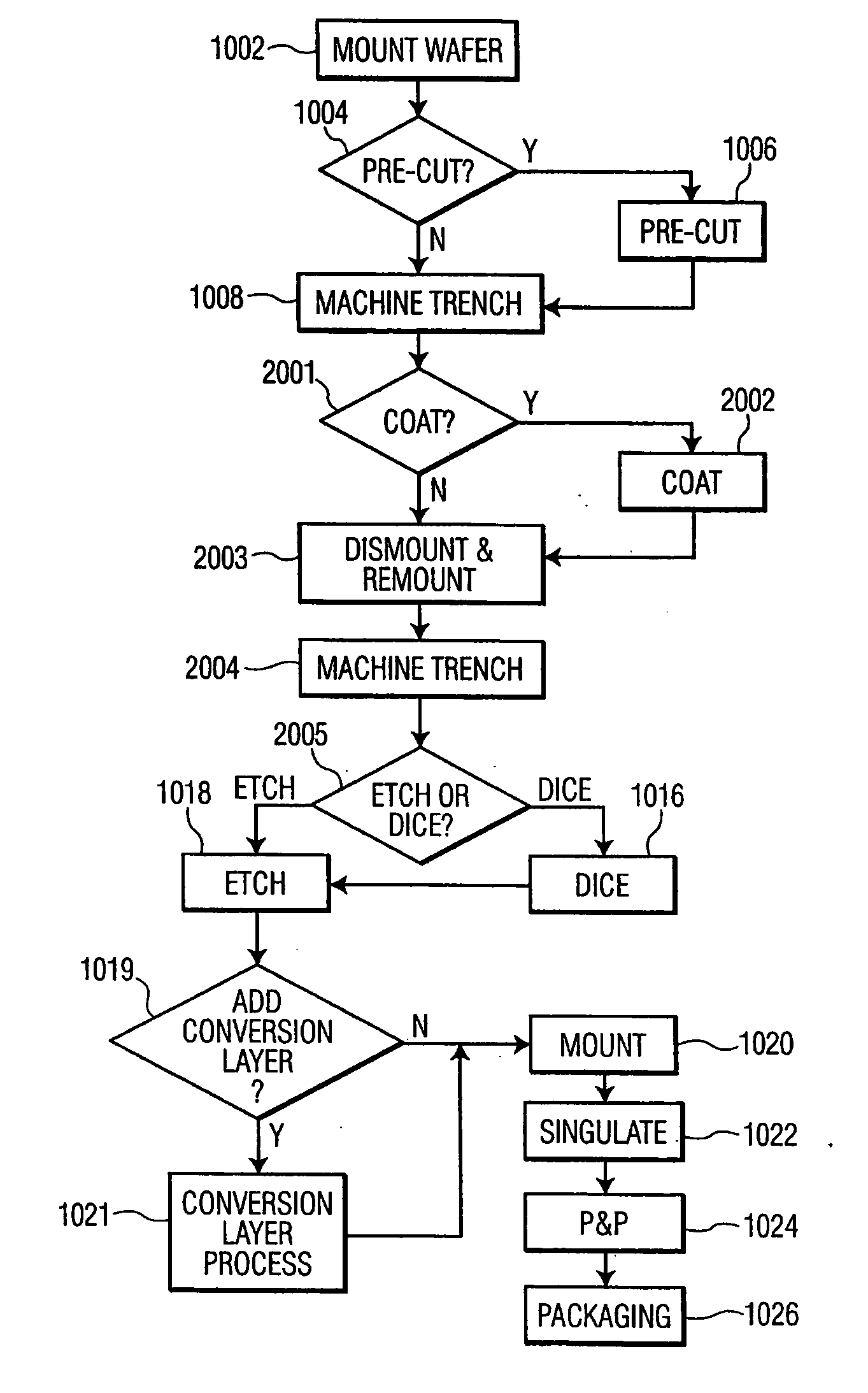
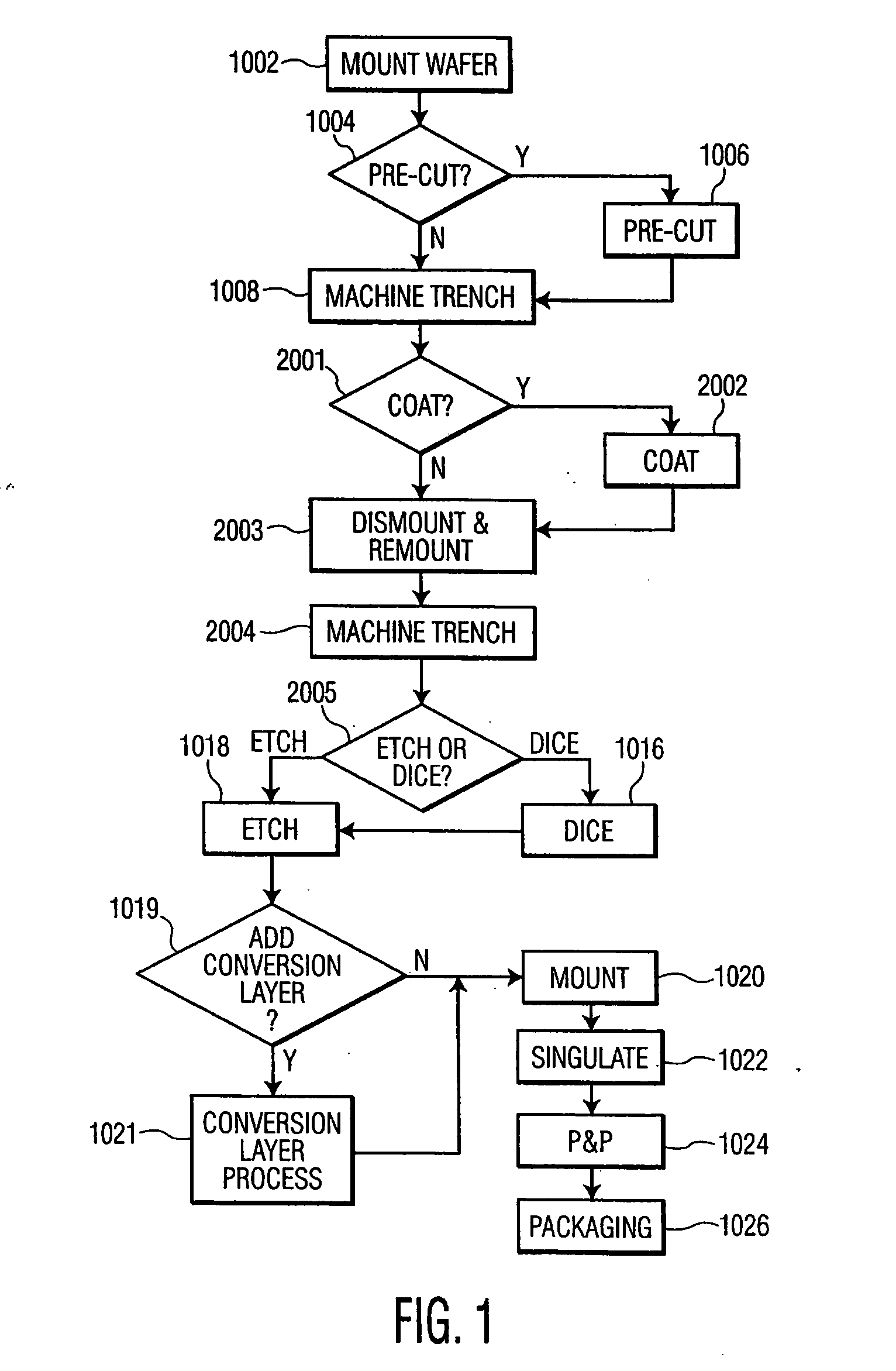
[0078]FIG. 1 illustrates a flow diagram of a method for manufacturing a double bevel surgical blade from silicon according to the present invention. The method of FIGS. 1, 2 and 3 generally describes processes which can be used to manufacture silicon surgical blades according to the present invention. However, the order of the steps of the method illustrated in FIGS. 1, 2 and 3 can be varied to create silicon surgical blades of different criteria, or to meet different manufacturing environments.
[0079] For example, although FIG. 1, as shown and described below, illustrates a method for manufacturing a double bevel blade in accordance with a first embodiment of the invention, this method can be utilized to manufacture multiple (i.e., three or more) facets per cutting edge. FIGS. 31A-C illustrate such a blade, and is described in greater detail below. Furthermore, the method as shown and described can also be utilized to manufacture a variable double bevel blade, as shown in FIG. 32. F...
second embodiment
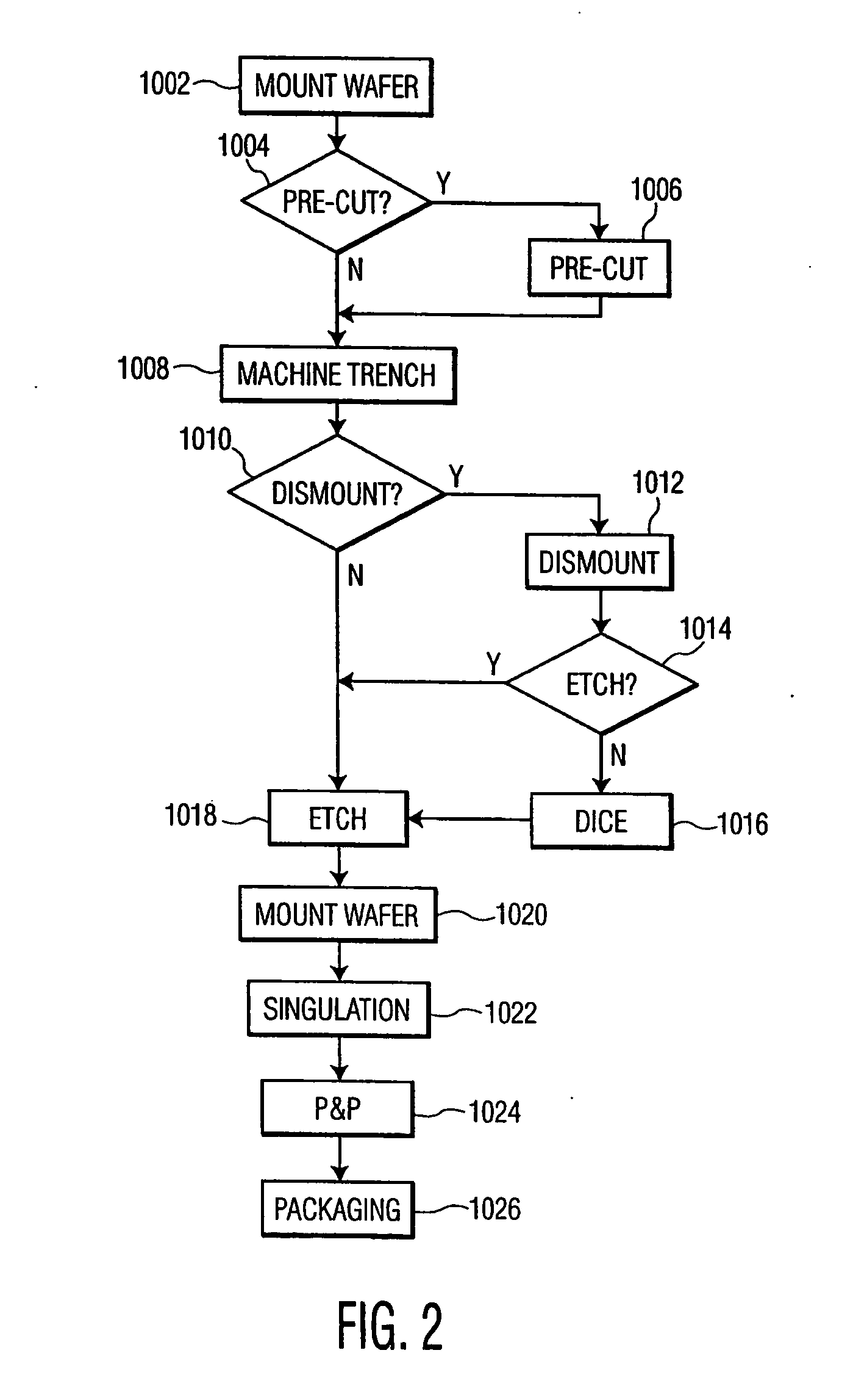
[0127] Having described the manufacturing process for a double bevel silicon-based surgical blade, attention is turned to FIG. 2, which illustrates a flow diagram of a method for manufacturing a single bevel surgical blade from silicon according to the present invention. Steps 1002, 1004, 1006, 1008 of FIG. 1 are the same for the method illustrated in FIG. 2, and therefore will not be repeated. However, the method for manufacturing a single bevel surgical blade differs in the next step, step 1010, from the method for manufacturing a double bevel blade, and therefore, will be discussed in detail.
[0128] Following step 1008 decision step 1010 determines whether the machined silicon wafer 202 will be dismounted from silicon wafer mounting assembly 204. If the single trench silicon wafers 202 were to be dismounted (in step 1012), then a further option is to dice the single trench wafers in step 1016. In optional dismounting step 1012, the silicon wafer 202 is dismounted from tape 308 uti...
third embodiment
[0130]FIG. 3 illustrates a flow diagram of an alternative method for manufacturing a single bevel surgical blade from silicon according to the present invention. The method illustrated in FIG. 3 is identical to that illustrated in FIG. 2, through steps 1002, 1004, 1006, 1008. After step 1008 in FIG. 3, however, there is coating step 2002. The coating step 2002 was described above in reference to FIG. 1, and need not be discussed in detail again. The result of the coating step is the same as was described previously: the machined side of silicon wafer 202 has a layer 1102 over it.
[0131] Following the coating step 2002, the silicon wafer 202 is dismounted and remounted in step 2003. This step is also identical as was previously discussed in reference to FIG. 1 (step 2003). The result is that the coated side of silicon wafer 202 is face down on the mounting assembly 204. Thereafter, steps 1018, 1020, 1022, 1024 and 1026 take place, all of which have been described in detail above. The ...
PUM
| Property | Measurement | Unit |
|---|---|---|
| Nanoscale particle size | aaaaa | aaaaa |
| Nanoscale particle size | aaaaa | aaaaa |
| Length | aaaaa | aaaaa |
Abstract
Description
Claims
Application Information


