Compound semiconductor device and manufacturing method thereof

a semiconductor device and manufacturing method technology, applied in semiconductor devices, semiconductor/solid-state device details, electrical devices, etc., can solve the problems of cracking on pad portions, increasing the number of processes and costs,

Inactive Publication Date: 2005-12-15
SANYO ELECTRIC CO LTD
View PDF15 Cites 26 Cited by
  • Summary
  • Abstract
  • Description
  • Claims
  • Application Information

AI Technical Summary

Problems solved by technology

Such an aspect may cause a lot of problems such as occurrence of damages by electrostatic discharge due to low insulation strength or deterioration in isolation due to leakage of a high frequency signal.
However, the nitride film is hard and therefore causes cracks on pad portions by pressure at the time of bonding.
However, a gold plating process causes increases in the number of processes and in costs.
The gold plating process causes increases in the number of processes and in costs.
For this reason, problems such as degradation in bonding adhesion or gouges on the substrate occur and lead to reduction in yields or deterioration in reliability.

Method used


Image

  • Compound semiconductor device and manufacturing method thereof
  • Compound semiconductor device and manufacturing method thereof
  • Compound semiconductor device and manufacturing method thereof

Examples


first embodiment

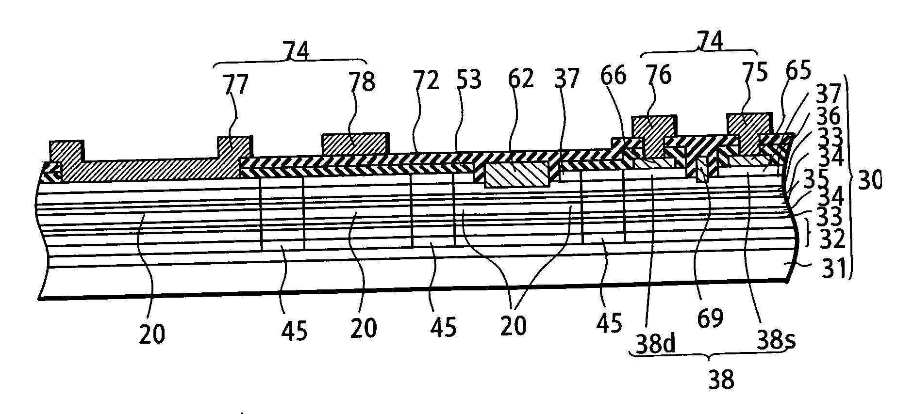
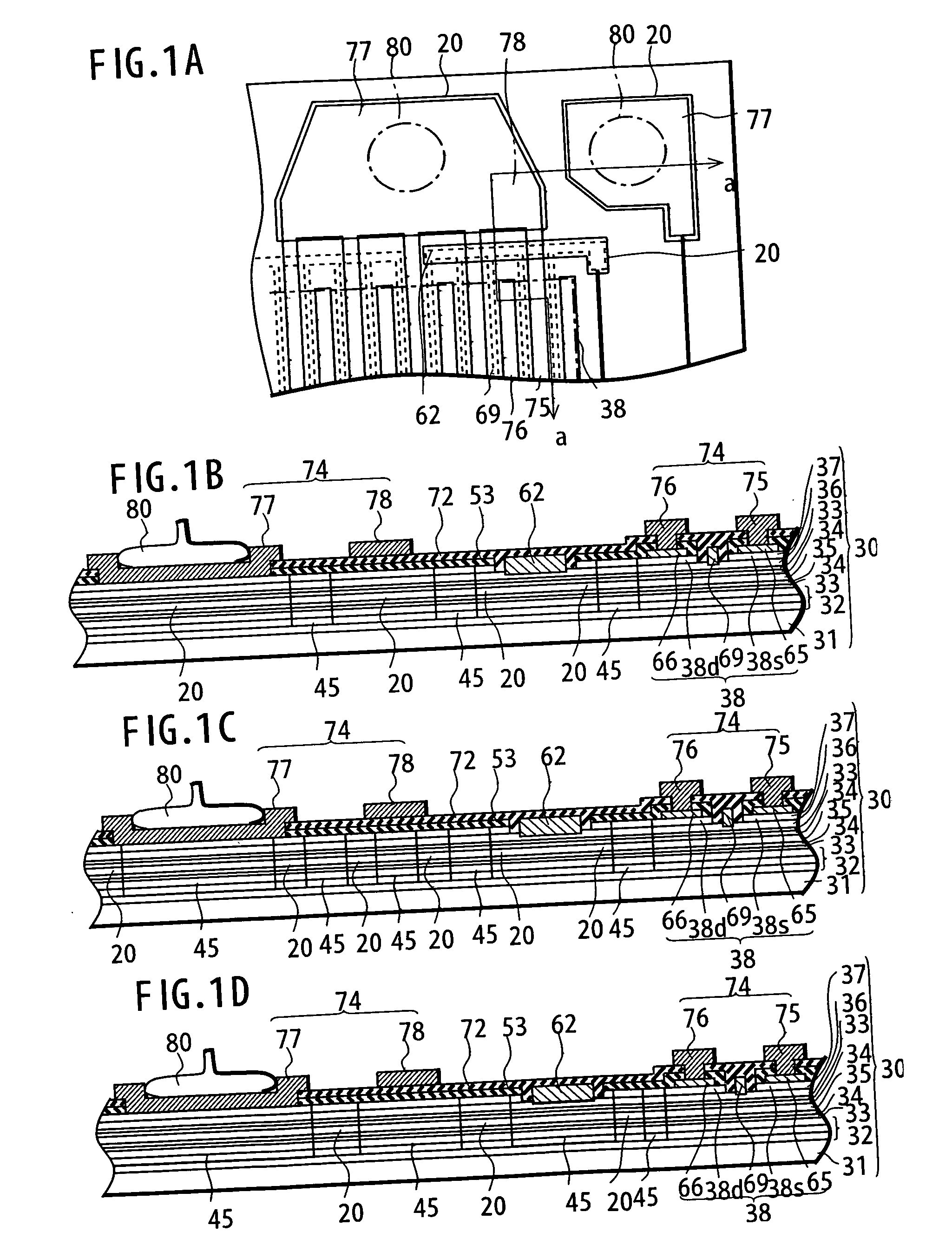
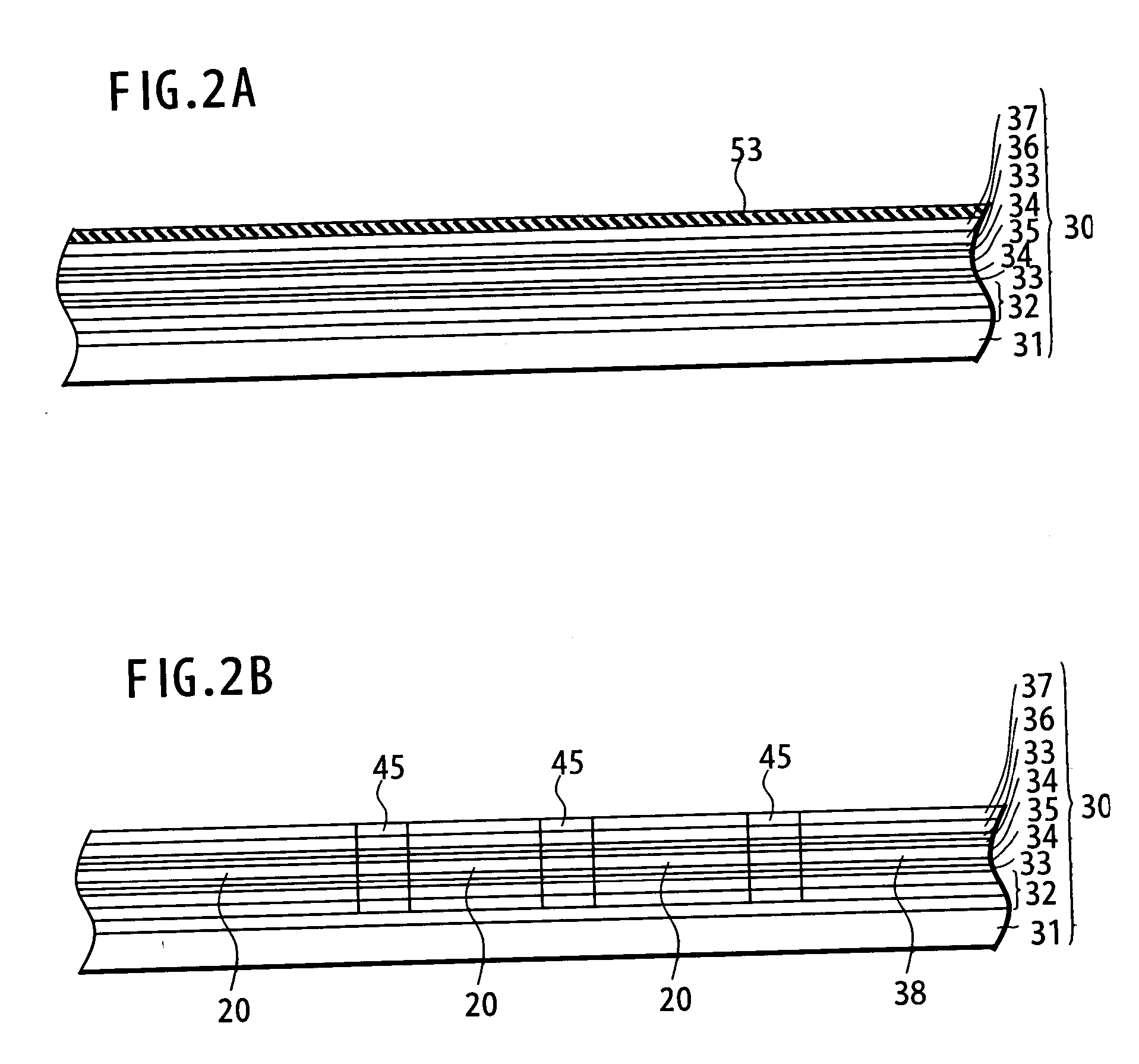
[0043]FIGS. 1A to 1D are views showing an example of a compound semiconductor device of the present invention, in which FIG. 1A is a plan view and FIG. 1B is a cross-sectional view taken along the a-a line. Here, the same formation elements as those in the conventional art are designated by the same reference numerals.

[0044] As shown in FIGS. 1A and 1B, concerning a method of forming substrate 30, first, undoped buffer layer 32 is grown on semi-insulating initial GaAs substrate 31. The buffer layer 32 is frequently formed as a plurality of layers. Then, n+-type AlGaAs layer 33 to be an electron supply layer, undoped InGaAs layer 35 to be an electron transimtting layer, and n+-type AlGaAs layer 33 to be another electron supply layer are sequentially grown on the buffer layer 32. Meanwhile, spacer layer 34 is disposed between the electron supply layer 33 and the electron transmitting layer 35.

[0045] Undoped AlGaAs layer 36 to be a barrier layer is grown on the electron supply layer 3...

second embodiment

[0111] That is, operating region 18 in the second embodiment is formed of source region 56 and drain region 57 formed by implanting ions of an n-type impurity (29Si+) into the n-type epitaxial layer 42, and of channel layer 52 between the both regions.

[0112] Then, ions of the n-type impurity (29Si+) are also implanted below the pad electrode 77, pad wiring 78, and gate wiring 62 to provide high concentration impurity region 60.

[0113] First source electrode 65 and first drain electrode 66 made of an ohmic metal layer 64 (AuGe / Ni / Au) of a first layer are provided on the source region 56 and the drain region 57.

[0114] Meanwhile, gate electrode 69 is provided by evaporating a gate metal layer (Pt / Mo) of a second metal layer to the channel layer 52. Moreover, second source electrode 75 and second drain electrode 76 made of pad metal layer 74 (Ti / Pt / Au) of a third metal layer are provided on the first source electrode 65 and the first drain electrode 66. Note that FIG. 6 shows one set o...


PUM

PropertyMeasurementUnit
distanceaaaaaaaaaa
thicknessaaaaaaaaaa
conductingaaaaaaaaaa

Abstract

A pad electrode of a high electron mobility transistor is formed solely of a pad metal layer without providing a gate metal layer. A high concentration impurity region is provided below the pad electrode, and the pad electrode is directly contacted to a substrate. Predetermined isolation is ensured by the high concentration impurity region. Accordingly, in a structure not requiring a nitride film as similar to the conventional art, it is possible to avoid defects upon wire boding attributing to hardening of the gate metal layer. Therefore, even in the case of a buried gate electrode structure for enhancing characteristics of the high electron mobility transistor, it is possible to enhance reliability and yields.

Description

BACKGROUND OF THE INVENTION [0001] 1. Field of the Invention [0002] The present invention relates to a compound semiconductor device and a manufacturing method of the same, particularly, to a compound semiconductor device and a manufacturing method of the same which are capable of enhancing characteristics of field effect transistors and reducing defects in wire bonding. [0003] 2. Background Art [0004] Mobile communication devices such as mobile telephones often use microwaves in a gigahertz range and frequently use switching devices to switch antennas or transmitting / receiving for switching those high frequency signals (see Japanese Patent Application Publication No. Hei 9-181642, for example). Such devices often use field effect transistors (hereinafter referred to as FETs) using gallium arsenide (GaAs) to deal with microwave signals. In this concern, development of monolithic microwave integrated circuits (MMICs) configured to integrate the above-mentioned switching circuits are ...

Claims


Application Information

Patent Timeline
Patent Type & Authority Applications(United States)
IPC IPC(8): H01L21/3205H01L21/336H01L21/338H01L21/60H01L21/768H01L21/822H01L23/52H01L23/485H01L23/522H01L27/04H01L27/06H01L27/095H01L29/778H01L29/812H01L31/0328H01L31/0336H01L31/072H01L31/109
CPCH01L24/03H01L24/05H01L2924/1306H01L2924/13064H01L2224/48669H01L2224/48666H01L2224/48644H01L2924/00014H01L2924/01023H01L2924/30107H01L2924/30105H01L2924/19043H01L2924/1423H01L2924/14H01L2924/10336H01L2924/10329H01L2924/05042H01L2924/01082H01L2924/01079H01L24/45H01L24/48H01L27/0605H01L29/7785H01L2224/04042H01L2224/05599H01L2224/05644H01L2224/05666H01L2224/05669H01L2224/45144H01L2224/48463H01L2924/01004H01L2924/01005H01L2924/01006H01L2924/01014H01L2924/01015H01L2924/01022H01L2924/01028H01L2924/01031H01L2924/01033H01L2924/01042H01L2924/01078H01L2924/01032H01L2924/00H01L2924/12032H01L2924/181H01L29/80
Inventor ASANO, TETSURO
Owner SANYO ELECTRIC CO LTD
Why Eureka
Try Eureka