Method for cleaning microstructure

Inactive Publication Date: 2005-12-22
KOBE STEEL LTD
View PDF25 Cites 22 Cited by
  • Summary
  • Abstract
  • Description
  • Claims
  • Application Information

AI Technical Summary

Benefits of technology

[0007] A method of the present invention comprises fluidizing a cleaning agent composition essentially containing carbon dioxide and a cleaning component under high pressure, and bringing the cleaning agent composition into a contact with a microstructure, for removing a substance adhering to the microstructure. The gist of the me

Problems solved by technology

Although the high-pressure carbon dioxide functions as a low-viscosity solvent, it has insufficient solvent power for pollutants and thus has insufficient cleaning power by itself.
However, as a result of further research carried out by the inventors, when a semiconductor wafer on which a low-dielectric-constant interlayer insulating film (Low-k film), which has been recently put in heavy use,

Method used


Image

  • Method for cleaning microstructure
  • Method for cleaning microstructure

Examples


Example

Experimental Example 1

[0035] An organic silicone MSQ raw material was applied to a Si wafer by a spin-on process and then dried to form a MSQ porous Low-k film. Then, a photoresist pattern for ArF is formed on the film, and exposure and development were performed to form a wafer sample having a resist pattern in which lines and spaces (width 130 nm) alternately appeared, and a wide pattern of about 10-μm square. The Low-k film was patterned by etching with fluorine-based gas and then subjected to ashing with hydrogen plasma to remove the resist. As a result of observation of the wafer surface after ashing, resist residue was observed on the lines and the wide pattern on which the resist had been applied.

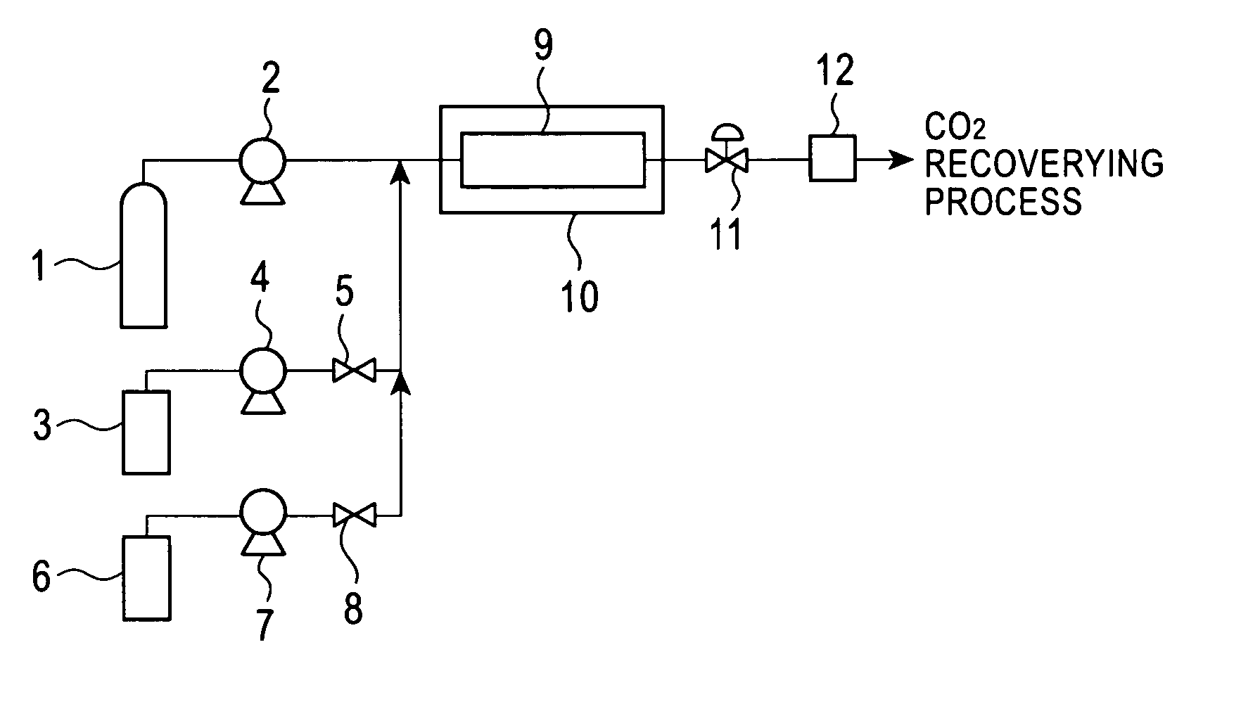
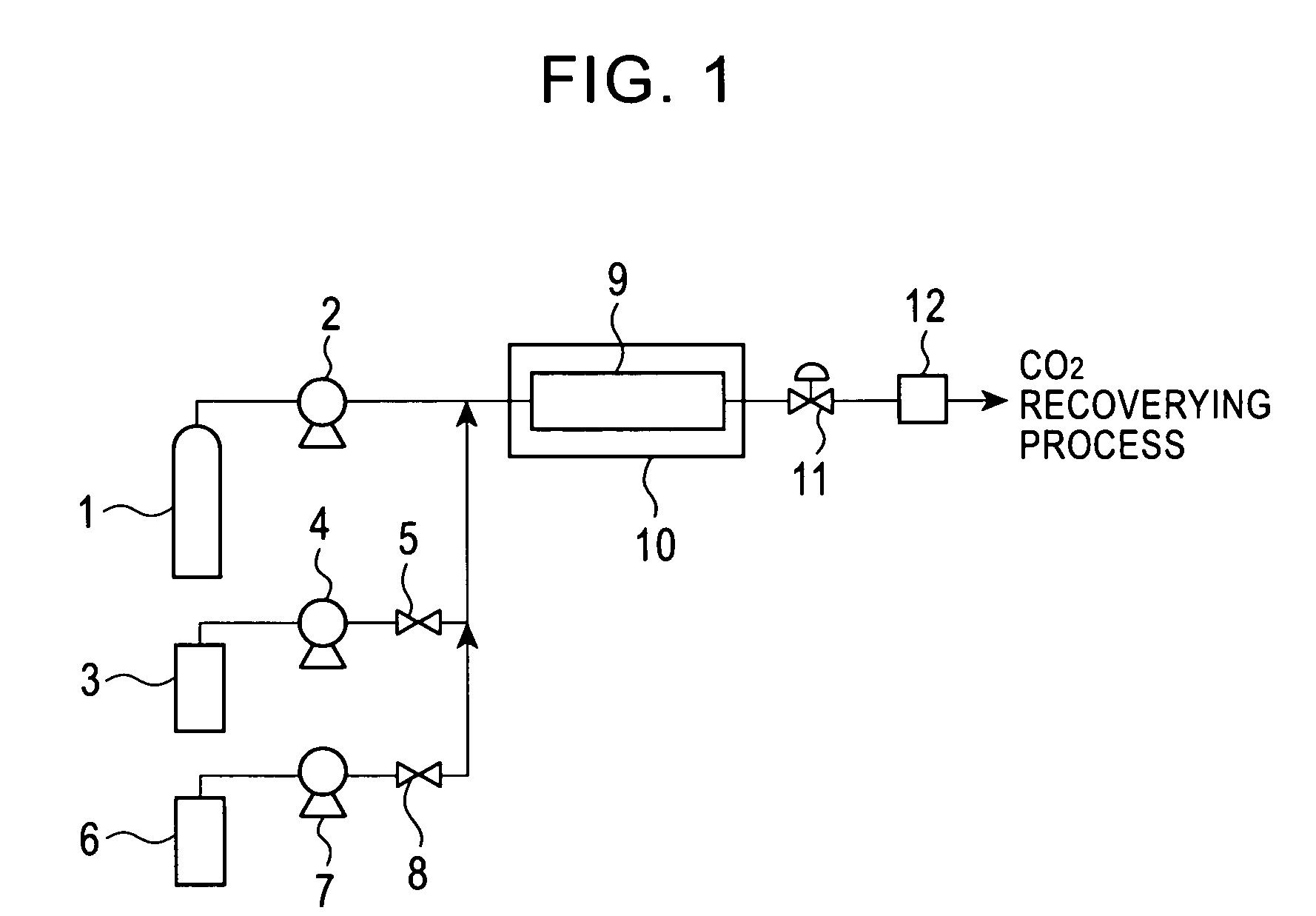
[0036] The sample after ashing was placed in the high-pressure vessel 9 in the apparatus shown in FIG. 1, and then the cover of the high-pressure vessel 9 was closed. Then, carbon dioxide was supplied to the high-pressure vessel 9 from the liquefied carbon dioxide cylinder 1 throug...

Example

Experimental Example 2

Comparative

[0050] Cleaning experiment (Run Nos. 19 and 20) was carried out by the same method as in Experimental Example 1 except that tetramethylammonium fluoride (TMAF) was used as a cleaning component in place of hydrofluoric acid. The results are shown in Table 2. TABLE 2Operating conditionCleaning agentCleaningEvaluation resultTemperaturePressurecomposition (% by mass)timeLow-kfilmRun(° C.)(MPa)CO2TMAFAlcohol(minute)DetergencyDamageResidue195015950.013EtOH4.9871AAB205015950.013EtOH4.9873ACB

Example

Example 3

Dielectric Constant

[0051] An organic silicone MSQ material was applied to a Si wafer by a spin-on process and then heated to form a MSQ porous Low-k film (dielectric constant=2.5). The wafer on which the porous Low-k film was deposited was cleaned with a cleaning agent composition containing 95% by mass of CO2, 0.01% by mass of HF, 0.01% by mass of H2O, and the balance composed of ethanol at an operating temperature of 50° C. and a pressure of 15 MPa for 1 minute. After cleaning, Al was vapor-deposited on the porous Low-k film and measured with respect to the dielectric constant. As a result, the dielectric constant k was 2.5.

[0052] Separately, a wafer on which a porous Low-k film was deposited was wet-cleaned with an aqueous ammonium fluoride solution (a commercially available aqueous solution of about 10% remover) for 1 minute, rinsed with ultrapure water, and then spin-dried by blowing nitrogen at room temperature. As a result of the measurement of the dielectric cons...


PUM

PropertyMeasurementUnit
Percent by massaaaaaaaaaa
Temperatureaaaaaaaaaa

Abstract

The present invention provides a method for cleaning a microstructure capable of efficiently removing pollutants such as resist residue without causing damage to a substance such as a low-k film which is necessary for a semiconductor wafer. The cleaning method includes fluidizing a cleaning agent composition essentially containing carbon dioxide and a cleaning component under high pressure, and bringing the cleaning agent composition into contact with a microstructure to remove a substance adhering to the microstructure, wherein hydrogen fluoride is used as the cleaning component.

Description

TECHNICAL FIELD [0001] The present invention relates to a method for cleaning a structure having a surface (microstructure surface) with micro irregularity, such as a semiconductor wafer, and for example, a cleaning method for removing resist residue and the like from a semiconductor wafer in a semiconductor manufacturing process. BACKGROUND ART [0002] A semiconductor manufacturing process frequently uses a step for forming a pattern using a resist. However, the resist unnecessary after being used for masking in etching is removed by ashing with oxygen plasma or the like (ashing step). Therefore, a cleaning step must be performed after the ashing step, for removing pollutants such as residue after the etching step and resist residue, which cannot be separated and removed from the wafer surface even by the ashing step. The cleaning step is an important step performed not only after the ashing step and performed frequently in the semiconductor manufacturing process. [0003] In recent y...

Claims


Application Information

Patent Timeline
IPC IPC(8): C23G1/02B08B3/00B08B7/00C23G1/00H01L21/02H01L21/304
CPCH01L21/02101H01L21/0206H01L21/304
Inventor MASUDA, KAORUIIJIMA, KATSUYUKI
Owner KOBE STEEL LTD
Why Eureka
Try Eureka