Passivation layer

a technology of organic light-emitting diodes and passivation layers, which is applied in the direction of discharge tubes/lamp details, organic semiconductor devices, discharge tubes luminescnet screens, etc., can solve the problems of thermally deposited cracks of most inorganic salts on cooling, and achieve the effect of few pinholes

Inactive Publication Date: 2006-01-12
MICROEMISSIVE DISPLAY
View PDF19 Cites 35 Cited by
  • Summary
  • Abstract
  • Description
  • Claims
  • Application Information

AI Technical Summary

Benefits of technology

[0010] We have found that when deposited in a film of suitable thickness, boron oxide (B2O3) is effective in protecting the device from subsequent deposition techniques such as electron beam deposition and sputtering. Importantly, boron oxide can be thermally deposited. Thermal deposition does not cause damage to the sensitive light emitting polymer or calcium layers. Boron oxide also has a very l...

Problems solved by technology

This is unusual, since most inorganic salts tha...

Method used


Image

  • Passivation layer
  • Passivation layer

Examples


Embodiment Construction

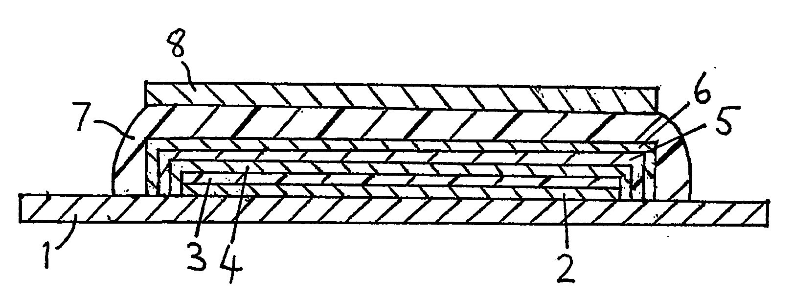
[0024]FIG. 1 shows a top-emitting PLED device comprising a silicon substrate 1, a nickel anode 2, a light emitting polymer layer 3 and a transparent calcium cathode layer 4.

[0025] A passivation layer 5 of boron oxide is deposited on the calcium layer 4 by thermal evaporation. This process comprises simply heating the boron oxide to evaporate it under a suitable vacuum and is the same process used for depositing the calcium layer 4. Boron oxide evaporates at about 1000° C. The thermal evaporation process does not damage the light emitting polymer layer 3 or the calcium layer 4.

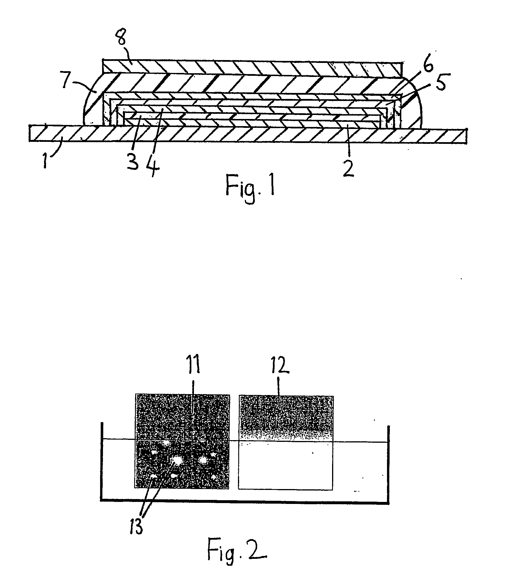
[0026] The boron oxide layer 5 is “conformal”, i.e. continuous without pinholes. This is demonstrated by FIG. 2, which shows the results of an experiment comparing silicon dioxide and boron oxide layers. Two test devices 11, 12, each comprised a glass substrate coated with a thin film of calcium. The first device 11 was then coated with a layer of silicon dioxide whilst the second device 12 was coated with a ...


PUM


Abstract

An organic light emitting diode device comprises a substrate (1), a layer (3) of organic, preferably polymeric, light emitting material, and a transparent cathode (4) comprising a layer of material with a work function less than 4 eV. The device has a passivation layer (5) comprising boron oxide.

Description

BACKGROUND OF THE INVENTION [0001] The present invention relates to an organic light emitting diode (OLED) device, a method of manufacturing an OLED device and a passivation layer for an electronic device. [0002] In particular, the OLED may be a polymer light emitting diode (PLED). PLEDs are usually fabricated on a conductive substrate such as of indium tin oxide (ITO) forming a transparent anode on to which layers of transparent conducting polymer, light emitting polymer, and cathode layers are deposited. A metal can, containing a getter to remove any water and oxygen, is glued over the device to encapsulate it. [0003] Such a “bottom-emitting” device is expensive and slow to manufacture and is bulky. [0004] Accordingly, “top-emitting” devices are also known, in which the substrate is opaque, for example a silicon wafer comprising active circuitry. In such devices, the light is emitted through the cathode, which must have very good electrical conductivity and transparency. Advantage...

Claims


Application Information

Patent Timeline
IPC IPC(8): H05B33/04H05B33/14H05B33/10H01L51/52
CPCH01L51/5237H05B33/04H01L2251/5315H10K50/828H10K50/8426H10K2102/3026H10K50/844
Inventor BUCKLEY, ALASTAIR ROBERT
Owner MICROEMISSIVE DISPLAY
Why Eureka
Try Eureka