Silicon wafer and method for manufacturing the same

a manufacturing method and silicon wafer technology, applied in the direction of polycrystalline material growth, crystal growth process, after-treatment details, etc., can solve the problems of bmds (bulk micro defects), circuit breakdown or other problems, micro defects, etc., to suppress the propagation of slip dislocations during annealing, suppress the effect of wafer strength reduction due to slip dislocations

Active Publication Date: 2006-01-26
SUMITOMO MITSUBISHI SILICON CORP
View PDF32 Cites 9 Cited by
  • Summary
  • Abstract
  • Description
  • Claims
  • Application Information

AI Technical Summary

Benefits of technology

[0026] According to the methods for manufacturing a silicon wafer of the second and third aspects, by forming the oxide film in at least the second surface, the oxide film in the second surface is exposed, thereby a decline in the oxygen concentration in the wafer during annealing is suppressed by the oxide film. Consequently, an oxygen concentration can be maintained which is sufficient to suppress propagation of the slip dislocations. Therefore, when the wafer is annealed in subsequent processes, the propagation of the slip dislocations during annealing can be suppressed. Hence, reductions in the wafer strength due to the slip dislocations can be suppressed, and silicon wafers can be obtained which have the DZ layer indispensable for device fabrication, and which retain high mechanical strength.

Problems solved by technology

In the case in which the crystal defects exist in the surface in which circuitry is formed, the defect portion may be the cause of circuit breakdown or other problems.
This supersaturated oxygen causes an occurrence of micro defects which are called BMDs (bulk micro defects) during annealing treatment in subsequent bulk processes.
However, in subsequent manufacturing or device fabrication entailing processes, there is a problem that when annealing a silicon wafer in which such a DZ (denuded zone) layer is formed, dislocation defects (slip) tend to occur within the wafer.
Particularly when annealing is performed in a state in which the wafer is supported by a heat treatment boat or similar, slip dislocations tend to propagate from the portions being supported on the rear surface of the wafer, resulting in a damage to the wafer during manufacturing processes, and possibly culminating in a destruction of the wafer.
However, because the silicon wafer in which the DZ layer is formed is in a state in which a oxygen concentration in the DZ zone is extremely low due to outward diffusion of oxygen, the wafer strength is inherently low, and in the case in which minute abrasions, dislocations, or the like occur during annealing processes in the course of device fabrication or the like, slip dislocations easily propagate.
Therefore, there is a problem that the occurrence of dislocation defects (slip) cannot be adequately suppressed merely by removal of the damage layer on the rear surface of the wafer.

Method used


Image

  • Silicon wafer and method for manufacturing the same
  • Silicon wafer and method for manufacturing the same
  • Silicon wafer and method for manufacturing the same

Examples


example 1

[0087] The inventors verified an influence of the DZ layer on a wafer strength (or slip dislocation). In order to perform the verification, the following wafers were prepared: a mirror-polished wafer prior to annealing (Sample 1); a wafer annealed at 1200° C. for one hour in Ar (Sample 2); a wafer which is annealed in Ar, followed by polishing to remove a portion of 10 μm thick from a rear surface (second surface) (Sample 3); and a wafer which is annealed in Ar, followed by polishing to remove a portion of 30 μm thick from a rear surface (Sample 4).

[0088] Resistivity of all the wafers was in a range from 3 to 11 Ω·cm. These wafers were subjected to heat treatment for thermal stress loading using a vertical furnace under a condition in which the wafers were set into the furnace at 900° C., temperature was ramped up at 10° C. / min to 1150° C., held at 1150° C. for 30 min, and ramped down at 3° C. / min to 900° C., and the wafers were removed at 900° C. A surface in contact with a heat t...

example 2

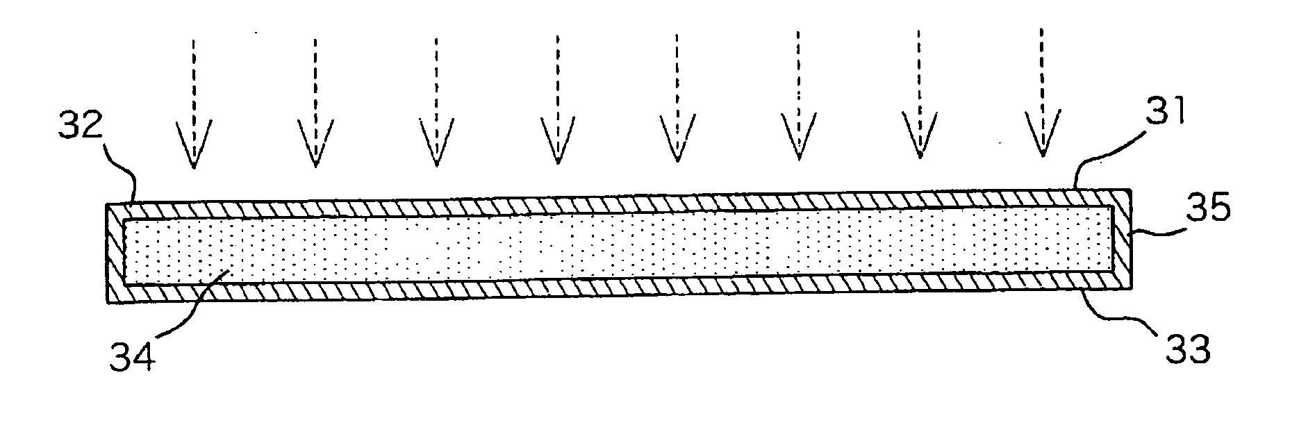
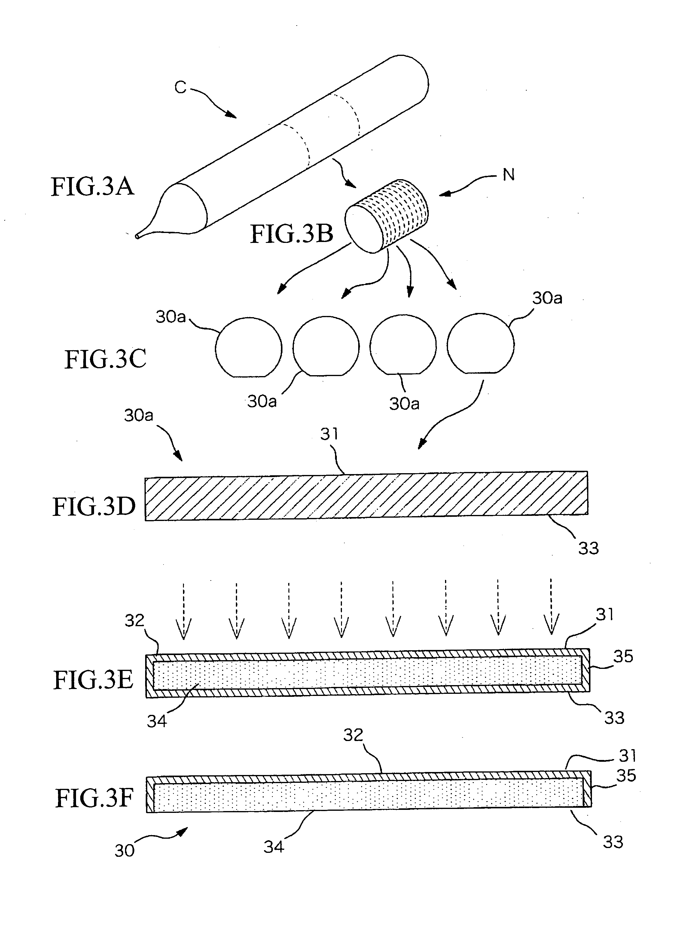
[0090] Next, the inventors verified a suppression of slip dislocations due to a formation of an oxide film. Outward diffusion of oxygen in an annealing process can also be prevented by forming the oxide film to protect the rear surface of the wafer prior to annealing. This is because the oxygen concentration at a surface interface between the oxide film and the silicon is constantly maintained at a thermal equilibrium concentration. At a temperature of 1150° C. or higher, the thermal equilibrium concentration of interstitial oxygen is approximately 8×10¹⁷ atoms / cc, and an effect to prevent propagation of slip dislocation can be expected. It is desirable that the oxide film formed before annealing has a thickness of 20 nm or thicker. The reason is as follows. In the case in which the thickness of the oxide film is thinner, the oxide film easily dissociates from the surface in heat treatment in a non-oxidizing atmosphere such as Ar or H2, however in the case in which the thickness is ...


PUM

PropertyMeasurementUnit
temperatureaaaaaaaaaa
thicknessaaaaaaaaaa

Abstract

A method for manufacturing a silicon wafer includes a step of annealing a silicon wafer which is sliced from a silicon single crystal ingot, thereby forming a DZ layer in a first surface and in a second surface of the silicon wafer and a step of removing either a portion of the DZ layer in the first surface or a portion of the DZ layer in the second surface.

Description

BACKGROUND OF THE INVENTION [0001] 1. Field of the Invention [0002] The present invention relates to a method for manufacturing a silicon wafer obtained by slicing a silicon single-crystal ingot produced by the Czochralski method, and to a technology appropriate for suppressing slip dislocations to improve wafer mechanical strength. [0003] The present invention contains subject matter related to Japanese Patent Application No. 2004-214983, filed on Jul. 22, 2004, the contents of which are incorporated herein by reference. [0004] 2. Description of the Related Art [0005] Single-crystal silicon wafers used as substrates for semiconductor devices and the like are manufactured by slicing a silicon single-crystal ingot and performing heat treatment, mirror polishing, and other processing. Methods for manufacturing such silicon single-crystal ingots include for example the Czochralski method (CZ method). Because the CZ method can be used to manufacture single-crystal ingots having large di...

Claims


Application Information

Patent Timeline
Patent Type & Authority Applications(United States)
IPC IPC(8): H01L21/322C30B15/14
CPCC30B29/06H01L21/3225C30B33/02
Inventor ONO, TOSHIAKISUGIMURA, WATARUHOURAI, MASATAKA
Owner SUMITOMO MITSUBISHI SILICON CORP
Why Eureka
Try Eureka