Laser diode arrays with reduced heat induced strain and stress

a technology of laser emitter and diode array, which is applied in the direction of lasers, laser details, electrical equipment, etc., can solve the problems of high heat generation, poor reliability of laser diode array, and large spectral emission, so as to improve reliability, improve power degradation, and improve the homogeneity and spectral performance of optical beams. , the effect of improving the defect impa

Inactive Publication Date: 2006-01-26
COMLASE
View PDF2 Cites 36 Cited by
  • Summary
  • Abstract
  • Description
  • Claims
  • Application Information

AI Technical Summary

Benefits of technology

[0021] Accordingly, an object of the present invention is to provide improved laser diode arrays.
[0022] Another object of the present invention is to provide laser diode arrays with improved reliability, optical beam homogeneity and spectral performance.
[0023] A further object of the present invention is to provide laser diode arrays with improved defect impact, power degradation and lower divergence of laser emitters.
[0024] Yet another object of the present invention is to provide laser diode arrays with reduced thermal gradients and hot-spots.
[0027] A further object of the present invention is to provide laser diode arrays that have a more uniform heat distribution which reduces heat induced strain and stress between the semiconductor and the heat sink of the laser diode array.
[0031] These and other objects of the present invention are achieved in a laser diode array with a semiconductor layered structure that includes at least one active layer. A heat sink is coupled to semiconductor layered structure. A plurality of laser emitters are formed in the active layer. A majority of the plurality of laser emitters have a spacing between adjacent laser emitters that provides for a more uniform heat distribution.

Problems solved by technology

Laser diode array performance and reliability are being plagued by very high heat generation in the laser emitters, broad spectral emission and poor beam quality.
High operating power densities, high operating temperatures of laser emitters of these laser arrays and high temperature differentials between emitter area and non-emitter area significantly reduce reliability, operating life time, operating efficiency and maximum power capability of the laser diode array itself.
This type of platform typically fails in industrial applications between only 4000 and 10,000 hours of operation, severely undermining the development of important applications such as pumping of kW class solid state lasers for automotive or electronic welding applications.
In addition, broad spectral emission reduces overall efficiency in important applications such as pumping of solid state lasers.
Meeting all these constraints limits the maximum continues wave (cw) output power from a laser diode array and its reliability and life time.
However, this heat sinking technology seriously limits the operating life time of the complete, practically useable, diode laser array platform.
Especially in important applications such as pumping of kW class solid state lasers for automotive and electronic welding, these platforms typically fail between 4,000 and 10,000 hours of operation.
One of the main failure modes is shearing and separation of the soft Indium solder, caused by frequent on / off cycling of the laser array, which is typical for welding applications.
Separation of the solder joint will locally impede heat removal, overheat the laser array and cause its failure.
Any leak in the cooler wall constitutes a failure of the array.
Erosion of internal structures, which guide the liquid flow to efficiently remove heat across the whole diode laser array surface, will lead to a change in flow patterns, localized overheating of the laser array, accelerated power degradation and premature failure.
Blockage of the small channels inside the micro cooler can also cause insufficient cooling of the laser array and premature failure.
One of the shortcomings of industry standard diode laser arrays with 90 μm to 200 μm emitter width, is that such highly transverse multimode emitters reduce focusability and depth of focus of the laser emission from each emitter.
Another shortcoming of current industry standard pump laser arrays for solid state laser pumping is that wavelength broadening causes manufacturing yield loss and raises cost for such diode laser arrays.
Furthermore, spectral broadening of the pump laser diode array emission causes additional, undesirable performance limitations for the solid state laser and requires application of costly temperature control mechanisms to prevent wavelength shift of pump diode laser arrays.
Pump laser radiation outside the absorption window is therefore wasted, causing reduced operating efficiency and excessive waste heat inside the crystal, which in turn leads to thermal lensing and stress and strain inside the crystal.
Thermal lensing and such internal stresses limit beam quality and maximum output power that can be obtained from such a solid state laser.
This type of wavelength broadening is one of the major contributors to manufacturing yield loss for diode laser arrays and forces diode laser pumped solid state lasers to employ costly temperature control mechanisms to maintain pump diode laser array wavelength inside the laser crystal absorption band.
Another problem with current, industry standard diode laser arrays arises from solder voids between the laser array and its heat sink.
One of the main difficulties is to mitigate voids in the solder used to attach the laser array to its respective heat sink.
Localized overheating inside a laser emitter can easily destroy the complete emitter, causing a sudden, premature power loss of the array between 2.7% and 5.3%, per each failing emitter.
If this defect is detected during the manufacturing process it will result in yield loss and raise manufacturing cost.
Otherwise, it will result in premature failure in its respective application, causing even greater loss and costs.
Inhomogeneities of the pump diode laser array light intensity distribution inside the solid state laser crystal will cause localized thermal lensing and stress and strain problems inside the solid state laser crystal, which degrade solid state laser beam quality and output power.
The wider the spacing of emitters and the wider the emitters of a pump laser diode array are, the more pronounced these problems become.

Method used


Image

  • Laser diode arrays with reduced heat induced strain and stress
  • Laser diode arrays with reduced heat induced strain and stress
  • Laser diode arrays with reduced heat induced strain and stress

Examples


Embodiment Construction

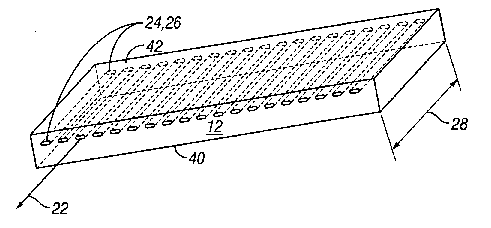
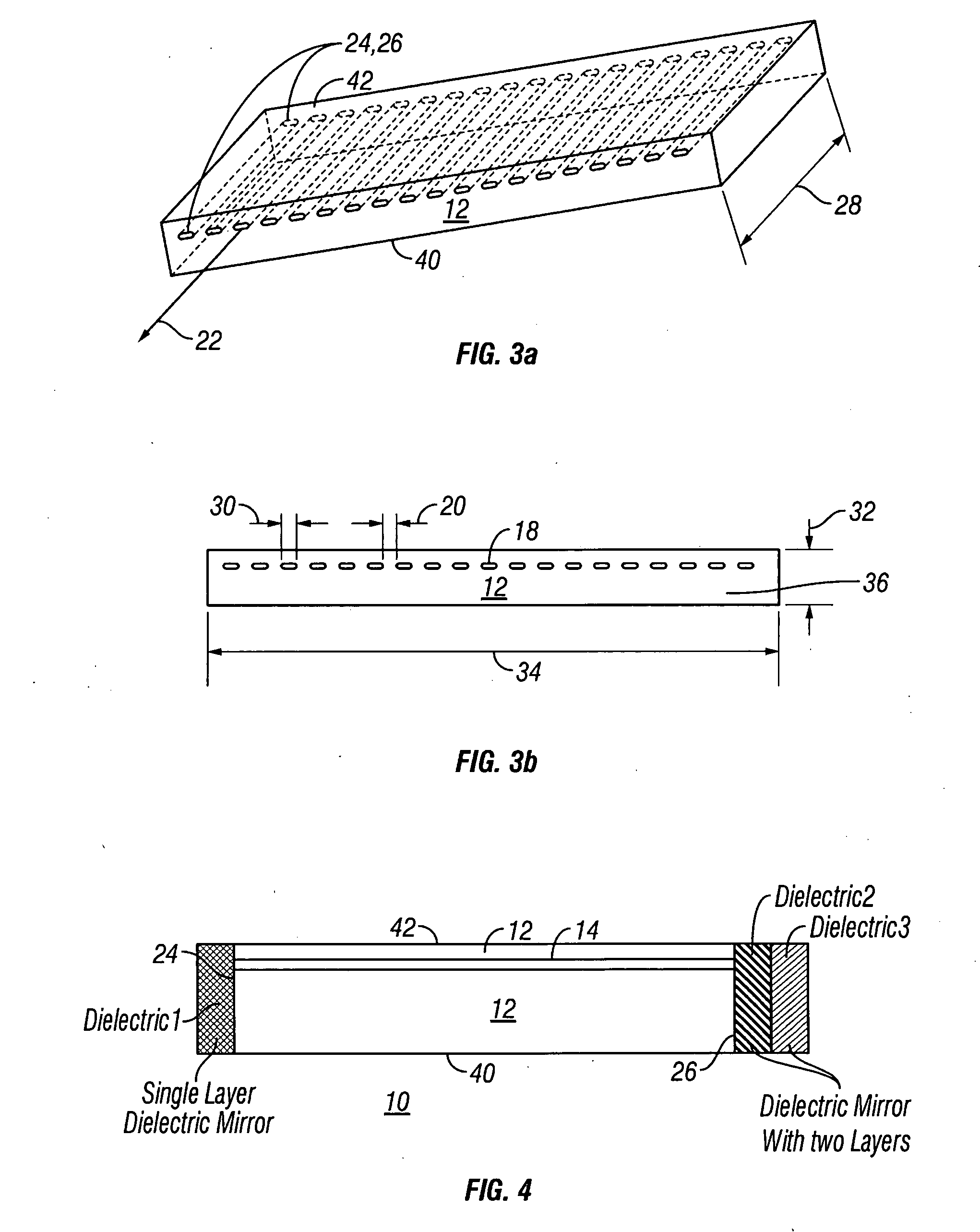
[0051] Referring to FIGS. 3(a) through 9(d), various embodiments of the present a laser diode array, generally denoted as 10, of the present invention, are illustrated. In one embodiment, laser diode array 10 includes a layered semiconductor structure 12 with at least one active layer 14. A heat sink 16 is coupled to layered semiconductor structure 12. A plurality of laser emitters 18 are formed in the at least one active layer 14. Laser emitters 18 each have a spacing 20 that is selected to provide for a more uniform heat distribution. In one embodiment, laser diode array 10 produces an output beam 22.

[0052] Emitters 18 can be spatially confined and localized lasers inside layered semiconductor structure 12 and includes laser mirrors. The laser mirrors are defined by two crystal mirror facets 24 and 26. The distance between crystal mirror facets 24 and 26 is the cavity length 28 of the laser, which can define one dimension of laser diode array 10. Each laser emits radiation from a...


PUM


Abstract

A laser diode array has a semiconductor layered structure that includes at least one active layer. A heat sink is coupled to semiconductor layered structure. A plurality of laser emitters are formed in the active layer. A majority of the plurality of laser emitters have a spacing between adjacent laser emitters that provides for a more uniform heat distribution.

Description

BACKGROUND OF THE INVENTION [0001] 1. Field of the Invention [0002] This invention relates generally to laser diode arrays, and more particularly to laser diode arrays that have a semiconductor and a heat sink and more uniform heat distribution in order to reduce heat induced strain and stress inside the semiconductor and between the semiconductor and the heat sink, reduce peak operating temperature inside the laser emitter and reduce broadening of the spectral emission. [0003] 2. Description of the Related Art [0004] Laser diode array performance and reliability are being plagued by very high heat generation in the laser emitters, broad spectral emission and poor beam quality. [0005] High operating power densities, high operating temperatures of laser emitters of these laser arrays and high temperature differentials between emitter area and non-emitter area significantly reduce reliability, operating life time, operating efficiency and maximum power capability of the laser diode ar...

Claims


Application Information

Patent Timeline
Patent Type & Authority Applications(United States)
IPC IPC(8): H01S5/00
CPCH01S5/02272H01S5/02423H01S5/4025H01S5/028H01S5/0281H01S5/02476H01S5/0237H01S5/02345
Inventor FEITISCH, ALFREDLINDSTROEM, CARSTENBLIXT, PETER
Owner COMLASE
Why Eureka
Try Eureka