
Laser crystallization apparatus and laser crystallization method

Inactive Publication Date: 2006-01-26
ADVANCED LCD TECH DEVMENT CENT
View PDF10 Cites 12 Cited by
  • Summary
  • Abstract
  • Description
  • Claims
  • Application Information

AI Technical Summary

Benefits of technology

[0019] The above-described problems can be solved by a laser crystall

Problems solved by technology

In the PMELA technique, in order to obtain a crystallized semiconductor film having a stabilized quality, it is one of important technical problems to constantly align a position of the non-single crystal semiconductor thin film being crystallized to an imaging position of the excimer laser light in every laser light irradiation for crystallization.
Therefore, substantial flatness of the substrate is generally worse than a focal depth of a laser optical system, for example, ±5 μm to 10 μm.
However, in the laser crystallization apparatus, as described later in detail, since crystallization laser light having high energy is used, lens temperature of an excimer imaging optical system rises during use, and it causes a shift in the imaging position of the excimer imaging optical system.
In a correction method using the conventional fixed substrate height measurement sensor, the shift of the imaging position caused by the laser crystallization apparatus itself due to the temperature change in the excimer imaging optical system cannot be corrected in principle.
However, if the shift is caused between the imaging position of the laser light and the position of the non-single crystal semiconductor thin film, then a predetermined light intensity distribution cannot be obtained on the non-single crystal semiconductor thin film.
As a result, a desired melting or crystallization of semiconductor film is not performed.
Additionally, the sizes of the crystal grains become nonuniform, thus the quality of the crystallized silicon film is degraded.
However, a constitution of an optical system including a laminated lens like a microscope lens for visible light is not applicable from the respect of heat resistance.
That is, a problem occurs that the imaging position shifts by the thermal lens effect.
As a result, there occur problems such as variation in image switching characteristic of the element formed therein, or a strained image.
However, correction for, for example, the shift of the imaging position caused by above-described thermal lens effect in optical system for excimer laser crystallization has not been considered.

Method used


Image

  • Laser crystallization apparatus and laser crystallization method
  • Laser crystallization apparatus and laser crystallization method
  • Laser crystallization apparatus and laser crystallization method

Examples


first embodiment

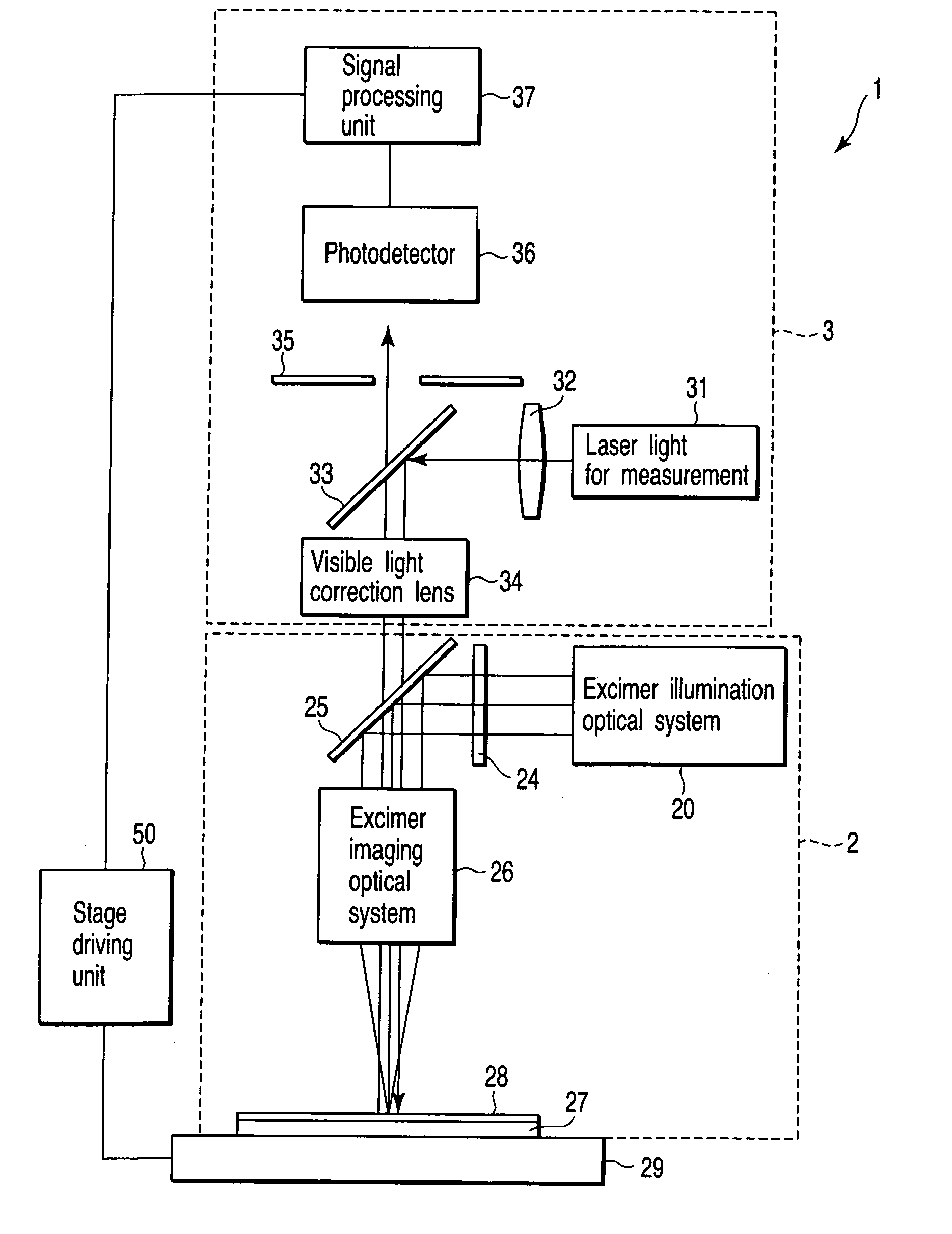
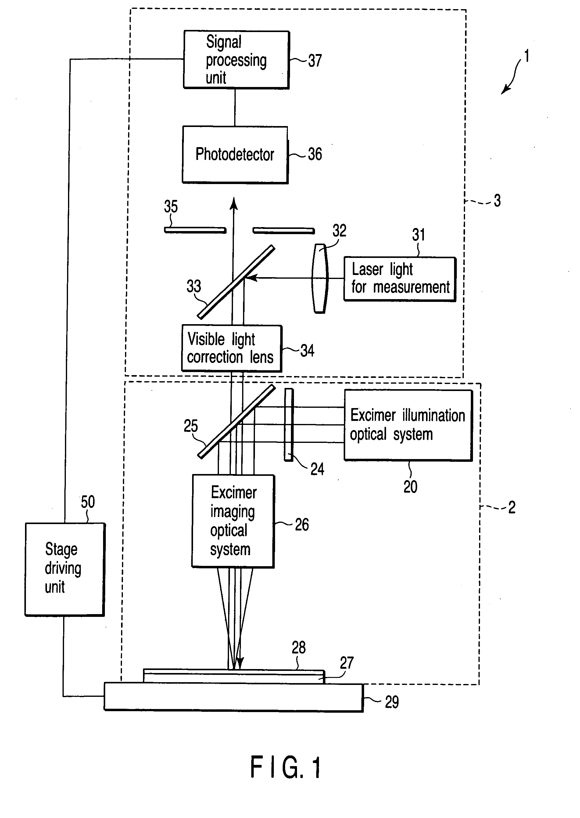
[0035]FIG. 1 is a schematic diagram of a laser crystallization apparatus 1 according to a first embodiment of the present invention. The apparatus is a laser crystallization apparatus 1 comprising a crystallization optical system 2 projecting an image of a phase modulating element 24 in a reduced size, and a substrate height correction system 3. The apparatus has a function for correcting a shift in a height direction of a substrate 27 to be crystallized based on measurement of the substrate height correction system 3.

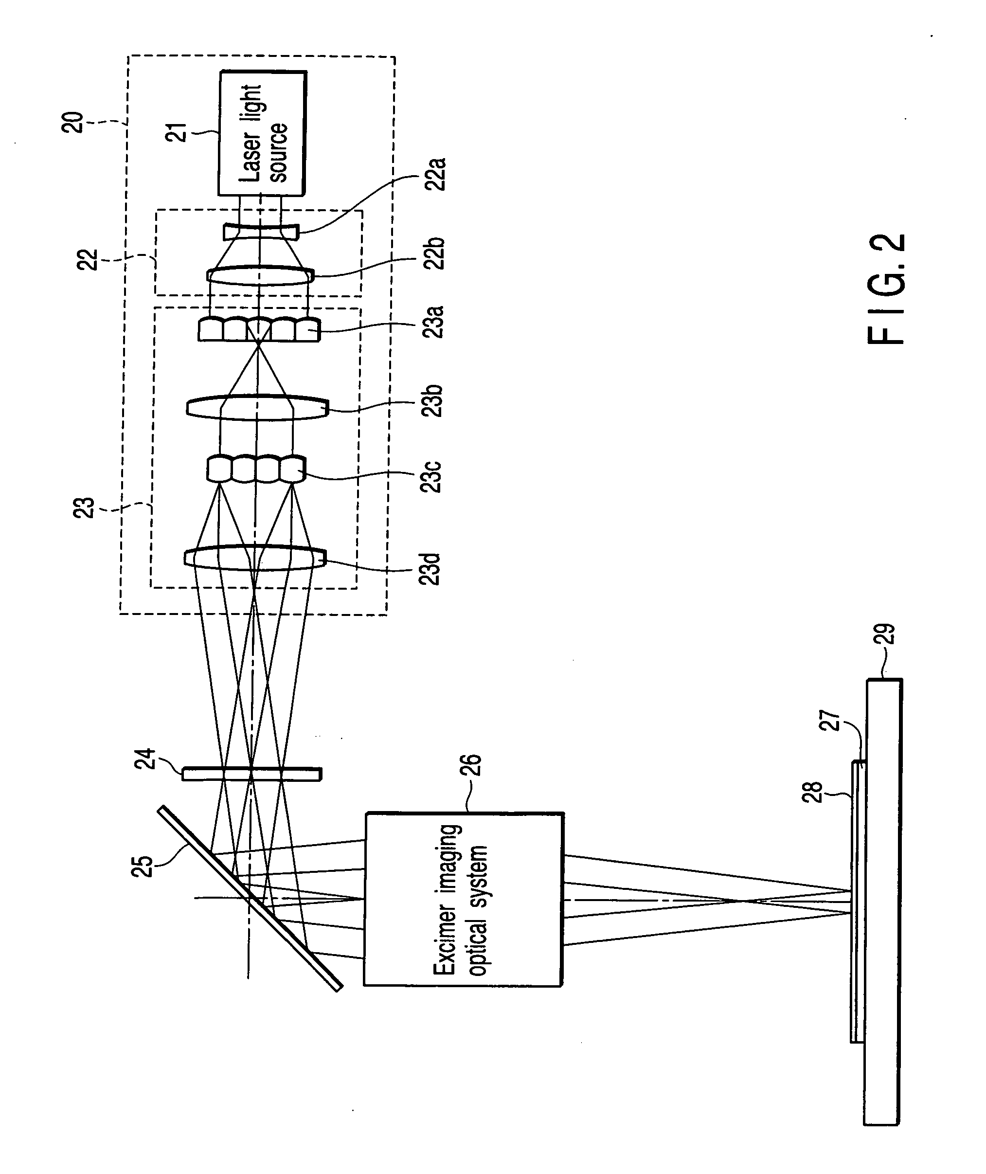
[0036] The crystallization optical system 2 comprises an excimer illumination optical system 20 and an excimer imaging optical system 26. The excimer illumination optical system 20 emits and conditions crystallization laser light which illuminates the phase modulating element 24, for example, a phase shifter. The excimer imaging optical system 26 irradiates crystallization laser light whose phase has been modulated by the phase shifter 24 onto a non-single crystal sem...

second embodiment

[0065] A second embodiment relates to a correction system 3 and method in which a specific mask pattern is imaged on a non-single crystal semiconductor film 28 on a substrate 27, a reflected image from the non-single crystal semiconductor film 28 is detected by a two-dimensional photodetector 36A, and then an imaging position is corrected using a two-dimensional image detected.

[0066] One example of the present embodiment is shown in FIG. 4. In FIG. 4, an optical system 2 for crystallization is the same as that in FIG. 1, and therefore a crystallization optical system 2 other than an excimer imaging optical system 26 is omitted. In the present embodiment, visible laser light from a light source 31 for measurement illuminates an image mask 42 having a predetermined pattern for measurement through an illuminating lens 41. The image of the mask pattern for the measurement is reflected on a half mirror 33, directed toward the substrate 27 to be crystallized, and imaged on the non-single...

third embodiment

[0073] A third embodiment relates to one example of a correction system capable of more precisely correcting a substrate position even if a change of lens temperature of an excimer imaging optical system 26 is large. Exactly speaking, a temperature coefficient of refractive index of a lens differs by wavelength of lights, i.e., temperature change in the refractive index of the lens differs for excimer laser light and visible laser light. In the present embodiment, the difference of the temperature change in refractive index of the lens caused by difference of wavelength of the light is further corrected.

[0074] The refractive index of the lens varies with the wavelength of light passed. For example, in calcium fluoride (CaF2), the refractive index for ultraviolet light having a wavelength of 0.2 μm is 1.4951, whereas the refractive index for visible light having a wavelength of 0.5 μm is 1.4365. The difference is about 4%. In fused silica for ultraviolet rays (UV-SiO2), the refracti...


PUM

PropertyMeasurementUnit
Heightaaaaaaaaaa
Distributionaaaaaaaaaa

Abstract

A laser crystallization apparatus which capable of correcting both shift in imaging position caused by thermal lens effect of the imaging optical system and shift due to flatness of the substrate comprises an crystallization optical system which irradiates laser light to a thin film disposed on the substrate to melt and crystallize an irradiated region of the thin film, the apparatus comprises a measurement light source which is disposed outside a light path of the laser light, and which emits measurement light being illuminated the irradiated region of the thin film, and a substrate height correction system which illuminates the thin film with the measurement light through an imaging optical system in the crystallization optical system, and which detects the reflected measurement light from the thin film.

Description

CROSS-REFERENCE TO RELATED APPLICATIONS [0001] This application is based upon and claims the benefit of priority from prior Japanese Patent Application No. 2004-214642, filed Jul. 22, 2004, the entire contents of which are incorporated herein by reference. BACKGROUND OF THE INVENTION [0002] 1. Field of the Invention [0003] The present invention relates to a crystallization apparatus which irradiates laser light to a thin film such as a semiconductor film and to a crystallization method, particularly to a laser crystallization apparatus comprising means for correcting positional shift of a semiconductor film with respect to an imaging position of laser light, and a laser crystallization method. [0004] 2. Description of the Related Art [0005] A laser crystallization technique for melting and crystallizing a non-single crystal semiconductor thin film using, for example, short pulse laser light having large energy is used to crystallize a semiconductor thin film used for manufacturing a...

Claims


Application Information

Patent Timeline
IPC IPC(8): H01L21/00
CPCB23K26/04B23K26/043H01L21/268H01S3/10
Inventor TAKAMI, YOSHIO
Owner ADVANCED LCD TECH DEVMENT CENT
Features
  • Generate Ideas
  • Intellectual Property
  • Life Sciences
  • Materials
  • Tech Scout
  • Unparalleled Data Quality
  • Higher Quality Content
  • 60% Fewer Hallucinations
Learn More