Method for manufacturing semiconductor device, and semiconductor device

a manufacturing method and semiconductor technology, applied in the direction of semiconductor devices, electrical apparatus, transistors, etc., can solve the problems of not sufficiently defining the use in mind, the margin for mask alignment, and the new objectives of ferams, etc., to achieve the miniaturization of the other element region, the effect of small occupancy area and low resistance between the second plug electrode and the third plug electrod

Inactive Publication Date: 2006-02-16
SEIKO EPSON CORP
View PDF5 Cites 28 Cited by
  • Summary
  • Abstract
  • Description
  • Claims
  • Application Information

AI Technical Summary

Benefits of technology

[0031] According to such a structure, the third opning section is provided on the wring that covers the second plug electrode, and not on the second plug electrode, such that a large margin can be given for mask alignment differences in photolithography. Also, the plug electrodes having a laminated structure in which the second plug electrode and the third plug electrode are stacked across the wiring pattern in a direction perpendicular to the substrate can be made to have a small occupancy area with respect to the substrate in a horizontal direction thereof, such that the plug electrodes having the laminated structure with the wiring patterns interposed between them can be densely arranged on the substrate. Accordingly, this can contribute to miniaturization of the other element region. Furthermore, by using a conductive material of low resistance such as aluminum for the wiring patterns, the resistance between the second plug electrode and the third plug electrode can be lowered.

Problems solved by technology

However, they are mainly used as embedded memories for microcomputers in which logic circuits are mix-mounted, and not as single purpose memory devices, which were expected at the beginning.
This is because only a few years have passed since FeRAMs' main use as memories for mix-mounted applications has became clear, and therefore what would be new objectives for FeRAMs when viewed with this use in mind have not been sufficiently defined.
However, the structure of directly stacking the plugs has a problem in that the process of forming via holes in the second interlayer dielectric film 370 allows only a small margin for mask alignment differences and therefore is highly difficult.
However, because the level of difficulty in micro-processing of ferroelectric capacitors including dummy capacitors is high and miniaturization lags behind, as compared with an ordinary logic circuit manufacturing process, contacts cannot be densely arranged by the method that uses dummy capacitors.
For this reason, in embedded memories in particular, miniaturization of logic regions can possibly be obstructed by the arrangement rule for dummy capacitors.
Furthermore, the method using dummy capacitors also has a problem in that an increase in contact resistance cannot be avoided because contacts are made through the lower electrode film.
Accordingly, the resistance of all wiring patterns connecting through the dummy capacitors is raised, which may possibly lead to a reduction in the operation speed of devices and an increase in the power consumption.

Method used


Image

  • Method for manufacturing semiconductor device, and semiconductor device
  • Method for manufacturing semiconductor device, and semiconductor device
  • Method for manufacturing semiconductor device, and semiconductor device

Examples


first embodiment

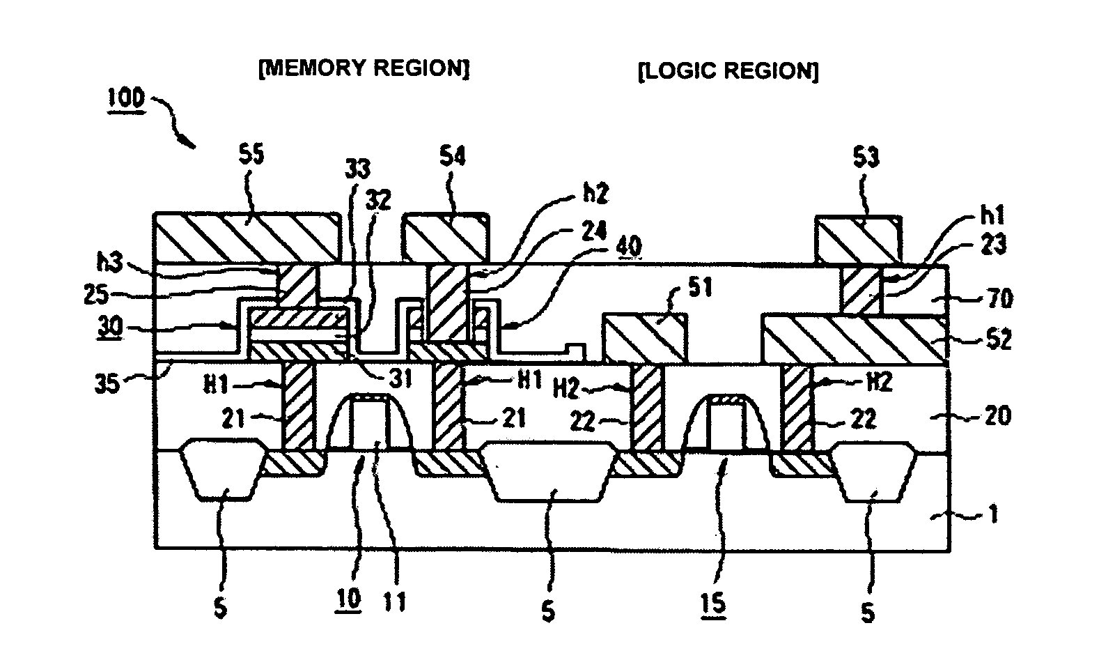
[0044]FIG. 1 is a cross-sectional view showing an exemplary structure of a semiconductor device 100 in accordance with the present invention. The semiconductor device 100 is a so-called embedded FeRAM that has a plurality of ferroelectric capacitors 30 in a memory region of a semiconductor substrate 1, and a logic circuit in a logic region of the semiconductor substrate 1.

[0045] As shown in FIG. 1, semiconductor device 100 includes a cell selection MOS transistor (i.e select transistor) 10 formed in the memory region of semiconductor substrate 1, a logic MOS transistor 15 formed in the logic region of semiconductor substrate 1, element isolation layers (i.e. isolation regions) 5, and a first interlayer dielectric film 20 provided over the semiconductor substrate 1. Semiconductor substrate 1 is, for example, a silicon substrate. As shown in FIG. 1, a plurality of first contact holes H1 that reach a surface of the semiconductor substrate 1 are provided in first interlayer dielectric f...

second embodiment

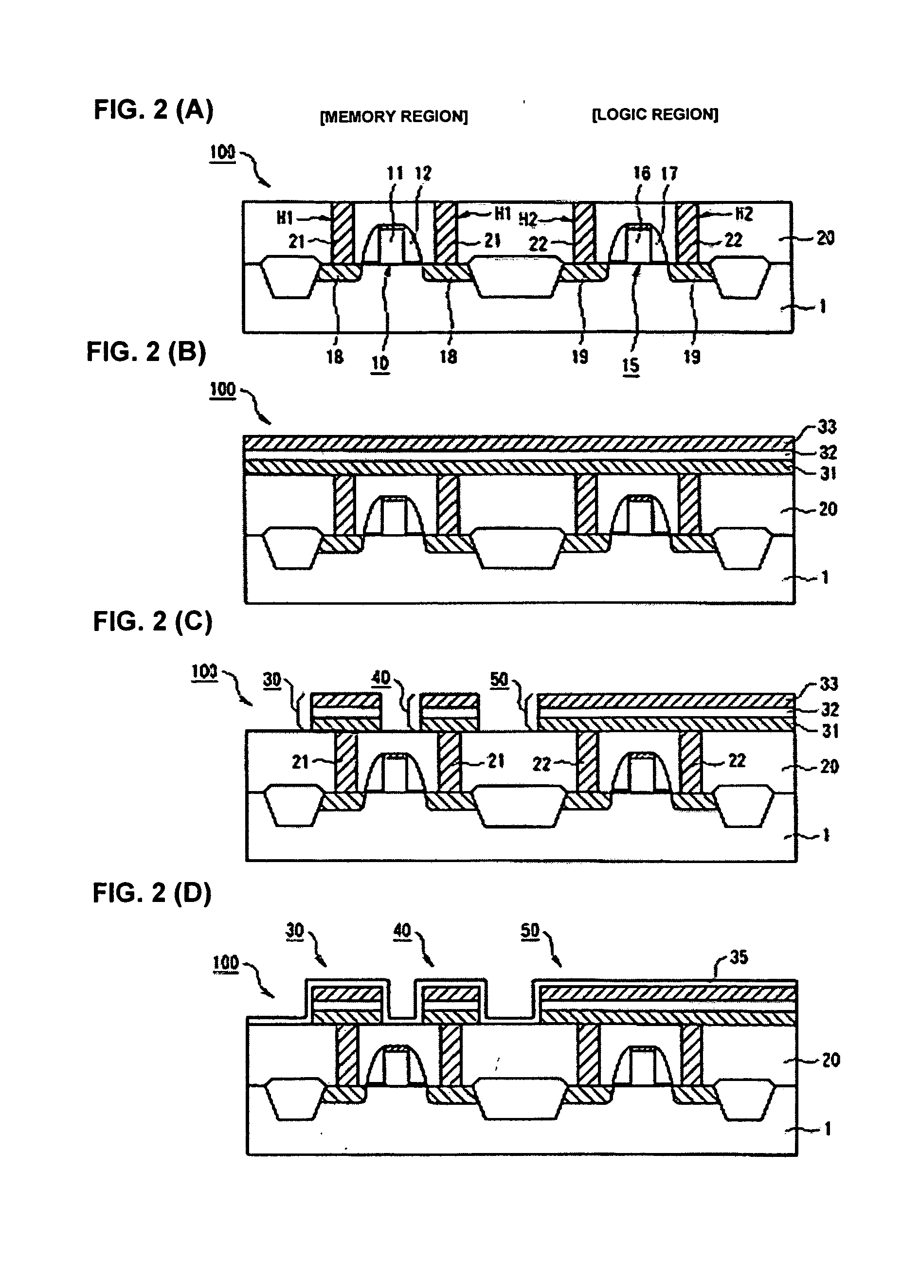
[0077]FIG. 4 is a cross-sectional view showing an exemplary structure of a semiconductor device 200 in accordance with the present invention. In FIG. 4, parts having substantially the same functions as those of the semiconductor device 100 shown in FIG. 1 are appended with the same reference numbers, and their detailed description is omitted. As shown in FIG. 4, the semiconductor device 200 includes a local wiring pattern 37 that extends from an area above the dielectric film 35 on the ferroelectric capacitor 30 to an area above dielectric film 35 at a position removed from the ferroelectric capacitor 30. Local wiring pattern 37 and the upper electrode 33 of the ferroelectric capacitor 30 are connected to each other. Also, local wiring pattern 37 is connected to a fifth plug electrode 25′ formed in a third via hole h′3 at a position removed from ferroelectric capacitor 30. Next, a method for manufacturing the semiconductor device 200 is described.

[0078] FIGS. 5(A) to 5(D) and FIG. 6...


PUM


Abstract

A manufacturing method for a semiconductor device that has a first region for memory elements and a second region for elements other than memory elements on a substrate, includes forming a first interlayer dielectric film on the substrate. A first opening section, which is made to reach the substrate, is formed in the first interlayer dielectric film over the first region. A second opening section, which also reaches the substrate, is formed in the first interlayer dielectric film over the second region. A first plug electrode is formed in the first opening section and a second plug electrode is formed in the second opening section. A ferroelectric capacitor is formed on the first interlayer dielectric film and made to cover and contact the first plug electrode. A first wiring pattern covering and contacting the second plug electrode is formed on the first interlayer dielectric film. A second interlayer dielectric film, which covers the ferroelectric capacitor and the first wiring pattern, is formed on the first interlayer dielectric film. A third opening section is then made in the second interlayer dielectric film over the second region and reaching the first wiring pattern. A third plug electrode is formed in the third opening section.

Description

RELATED APPLICATIONS [0001] Japanese application No. 2004-235230 is hereby incorporated by reference in its entirety. BACKGROUND OF THE INVENTION [0002] 1. Field of the Invention [0003] The present invention relates to methods for manufacturing semiconductor devices and to semiconductor devices, and more particularly relates to a method for manufacturing an embedded FeRAM in which a ferroelectric capacitor and a logic circuit are mix-mounted (i.e. constructed on the same integrated circuit, IC), and a method for manufacturing the same. [0004] 2. Description of the Related Art [0005] Conventionally, ferroelectric memories (FeRAMs: ferroelectric memories) have been widely known as nonvolatile memories using polarization hysteresis characteristics of ferroelectric materials. Because FeRAMs are capable of operating with low power consumption and at high speed, demand for FeRAMs is growing. Miniaturization and higher-integration of such FeRAMs are advancing like other memory devices such...

Claims


Application Information

Patent Timeline
Patent Type & Authority Applications(United States)
IPC IPC(8): H01L29/76
CPCH01L27/11507H01L27/11502H10B53/30H10B53/00
Inventor FUKADA, SHINICHI
Owner SEIKO EPSON CORP
Why Eureka
Try Eureka