Method of fabricating planarized poly-silicon thin film transistors

a thin film transistor and polysilicon technology, applied in the direction of basic electric elements, electrical apparatus, semiconductor devices, etc., can solve the problems of gate oxide layer breakdown, poor influence on the electrical properties of devices, and the normal surface of poly-si, so as to increase the electrical properties and reliability of tft devices, reduce the number of steps in the method, and reduce the average roughness of the poly-si surface

Inactive Publication Date: 2006-03-09
IND TECH RES INST
View PDF4 Cites 10 Cited by
  • Summary
  • Abstract
  • Description
  • Claims
  • Application Information

AI Technical Summary

Benefits of technology

[0011] In accord with the above object, the invention provides a method of fabricating planarized poly-Si TFF's. A buffer layer, a protective layer and a poly-silicon layer are formed in sequence on a substrate. The buffer layer is made of, for example, silicon oxide. The protective layer uses an insulating material that is resistive to the silicon oxide etching environment. It has to have a high etching selection ratio relative to silicon oxide, e.g. silicon nitride and SiOxNy, to protect the buffer from the damages of silicon oxide in the subsequent planarization process. Besides, the poly-Si layer can be formed directly by chemical vapor deposition (CVD) of poly-Si or first depositing an amorphous (a-Si) layer and then turning the a-Si layer into a poly-Si layer by laser crystallization.
[0013] After defining island active regions and implanting ions, the poly-Si layer undergoes a surface planarization process. The surface of the poly-Si surface is micro-etched to change its surface morphology. Afterwards, a laser annealing process is performed to partially melt the poly-Si layer for forming a smoother surface and activating the source / drain regions on the poly-Si layer simultaneously. The micro-etching step involves a wet etching that uses a buffer oxide etchant to remove the native oxide layer on the poly-Si surface and the part with weaker bonds in the poly-Si lattice. This achieves the effect of reducing the surface roughness. The laser beam energy used in the laser annealing process is lower than the laser crystallization energy for melting the poly-Si layer, e.g. 200˜350 mJ / cm2. Therefore, it can achieve the simultaneous effects of planarizing the surface of the poly-Si layer and activating the source / drain regions on the poly-Si layer.
[0016] Since the invention can combine the surface planarization and source / drain region activation together in the same laser process, the number of steps in the method is reduced. This is particularly convenient for making N-type TFT devices that require activation.
[0017] According to the disclosed method, the average roughness of the poly-Si surface is efficiently reduced down to below 30 Å. Therefore, the disclosed fabrication method can not only greatly increase the electrical properties and reliability of TFT devices, but also helps improving the quality in the subsequent fabrication of thin film layers and increasing the production yield.

Problems solved by technology

However, aside from the control in grain sizes, an existing technical problem in fabricating poly-Si TFT's is that the surface of poly-Si is normally too rough.
This will have bad influences on the electrical properties of devices.
The ridge part of the poly-Si layer is likely to have a large electric field, causing the breakdown of the gate oxide layer and enlarging the leak current.
For devices that have special requirements for the thin gate oxide layers, the above-mentioned problems are more serious.
Moreover, in the photolithography process, the roughness of the poly-Si surface will result in random scattering during the exposure and thus errors in size definitions.
Therefore, the rough surface of poly-Si does not only have poor effects on the electrical properties of the device, it also lowers the product yield of the TFT devices.
Although there are literatures and patents pointing out methods to improve the rough poly-Si surface using the chemical mechanical polishing (CMP) process, this cannot be applied to fabricate large-area displays.
Moreover, this method can only achieve limited improvement in the surface roughness of poly-Si, with an average roughness of 30˜40 angstrom (Å).
Therefore, the method is not suitable for the trend in recent years to make large-area displays and smaller devices.
However, directly applying this method in the fabrication of the TFT devices requires the additional laser process.
In particular, for the N-type metal oxide semiconductor (MOS) TFT that needs to go through an activation process, there involve even more steps and a higher production cost.

Method used


Image

  • Method of fabricating planarized poly-silicon thin film transistors
  • Method of fabricating planarized poly-silicon thin film transistors
  • Method of fabricating planarized poly-silicon thin film transistors

Examples


embodiment

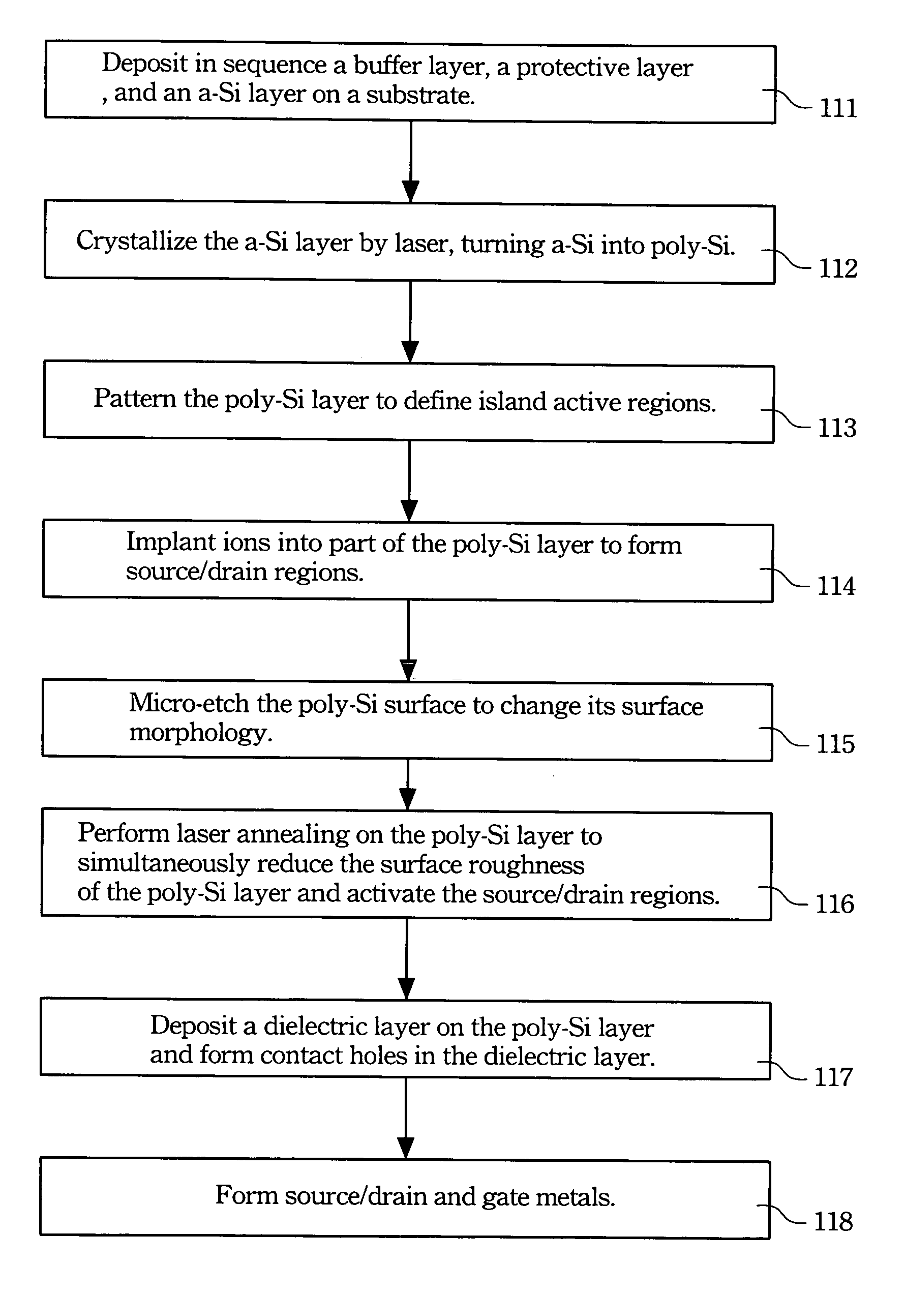
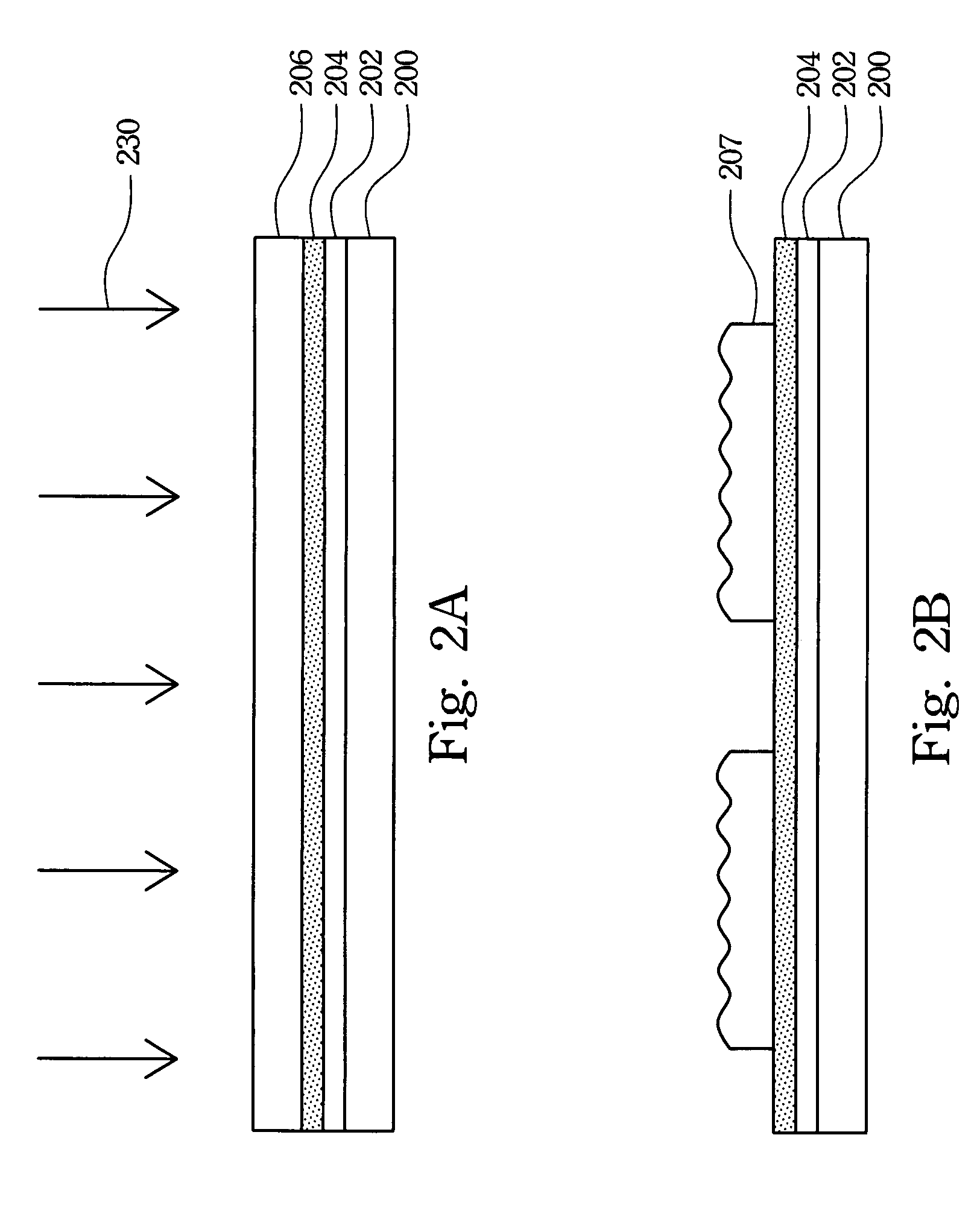
[0023] The disclosed method of fabricating planarized poly-Si TFT's is illustrated in FIGS. 1 and 2A to 2F. FIG. 1 shows the flowchart of the method according to the preferred embodiment. FIGS. 2A to 2F are schematic cross-sectional views of fabricating the planarized poly-Si TFT.

[0024] This embodiment uses the fabrication of an N-type TFT as an example. First, step 111 in FIG. 1 is performed to deposit on a substrate 200 in sequence a buffer layer 202, a protective layer 204, and an a-Si layer 206, as shown in FIG. 2A. For the production of displays, the substrate 200 can be glass, the buffer layer 202 can be a silicon oxide layer, and the protective layer 204 can be an insulating material that is resistive to a silicon oxide etching environment. Such an insulating material, such as silicon nitride (SiNx) and SiOxNy, has a high etching selection ratio than silicon oxide to protect the buffer layer 202. Therefore, in subsequent planarization of the poly-Si surface, the buffer layer...


PUM

PropertyMeasurementUnit
thicknessaaaaaaaaaa
roughnessaaaaaaaaaa
roughnessaaaaaaaaaa

Abstract

A buffer layer, a protective layer and a poly-silicon layer are formed on a substrate in turn, and the poly-silicon layer is then patterned to form island active regions. Next, n-type ions are implanted into portions of the poly-silicon layer to form source / drain regions. Then, a dilute buffer oxide etchant is utilized to micro-etch the poly-silicon layer to change the surface morphology of the poly-silicon. Finally, a laser annealing process is performed to partially melt the poly-silicon for forming a smooth surface and activating the source / drain region of the poly-silicon simultaneously.

Description

RELATED APPLICATIONS [0001] The present application is based on, and claims priority from, Taiwan Application Serial Number 93127021, filed Sep. 7, 2004, the disclosure of which is hereby incorporated by reference herein in its entirety. BACKGROUND OF THE INVENTION [0002] 1. Field of Invention [0003] The invention relates to a method of fabricating poly-silicon thin film transistors and, in particular, to a method of fabricating planarized poly-silicon thin film transistors. [0004] 2. Related Art [0005] Thin film transistors (TFT) have been widely used for driving active liquid crystal displays (LCD). In particular, the poly-silicon (poly-Si) TFT apparently has a higher electron mobility and thus receives much attention in the applications of LCD in recent years. The advantage of the poly-Si TFT is the ability of making a display with a fast response speed and a high resolution. It is particularly suitable for integrating a driving circuit onto the display panel. [0006] However, asi...

Claims


Application Information

Patent Timeline
Patent Type & Authority Applications(United States)
IPC IPC(8): H01L21/84H01L21/00
CPCH01L21/2026H01L27/1285H01L29/66757H01L21/32134H01L21/02675H01L21/02532
Inventor CHEN, HUNG-TSECHEN, YU-CHENGCHEN, CHI-LIN
Owner IND TECH RES INST
Why Eureka
Try Eureka