Substrate for epitaxy and method of preparing the same

a technology of substrates and epitaxy, which is applied in the direction of crystal growth process, polycrystalline material growth, transportation and packaging, etc., can solve the problems of substrate epitaxy face area decrease, density is still too high to ensure the correct functioning of many electronic and opto-electronic devices

Active Publication Date: 2006-03-16
AMMONO SP Z O O (PL) +1
View PDF10 Cites 66 Cited by
  • Summary
  • Abstract
  • Description
  • Claims
  • Application Information

AI Technical Summary

Benefits of technology

[0013] According to the present invention, as shown in FIG. 7B, a substrate having a thickness of 100 to 300 μm or more can be obtained from a portion of the layer B2) in the combination layers of A) the layer of bulk mono-crystal nitride containing at least one element of alkali metals (Group I, IUPAC 1989), B1) the layer of nitride grown by means of MOCVD or MBE and B2) the layer of gallium-containing nitride grown by means of HVPE. The resulting template can consist of substantially complete Ga-polar face area at one of sides of the substrate, that is, more than 95%, preferably more than 99% of Ga-polar face. In comparison with HVPE GaN substrate made by the ELOG method having less than 90% of Ga-polar face area because of some of N-polar face area on the same surface, there is obtained a substrate having an excellent quality as to the dislocation density and FWHM of the X-ray rocking curve as well as the complete Ga-polar face.
[0014] According to a second aspect of the present invention, a template type substrate may comprise the layer A) of bulk mono-crystal nitride prepared on a seed having the layer B) by crystallization of nitride in a supercritical ammonium solution containing at least one element of alkali metals. In this case, the templ

Problems solved by technology

Therefore, there have been proposed an application of ELOG-type structures to the substrate, which allows to decrease the dislocation density down to 106/cm2, but that density is still too high to ensure the correct functioni

Method used


Image

  • Substrate for epitaxy and method of preparing the same
  • Substrate for epitaxy and method of preparing the same
  • Substrate for epitaxy and method of preparing the same

Examples


example

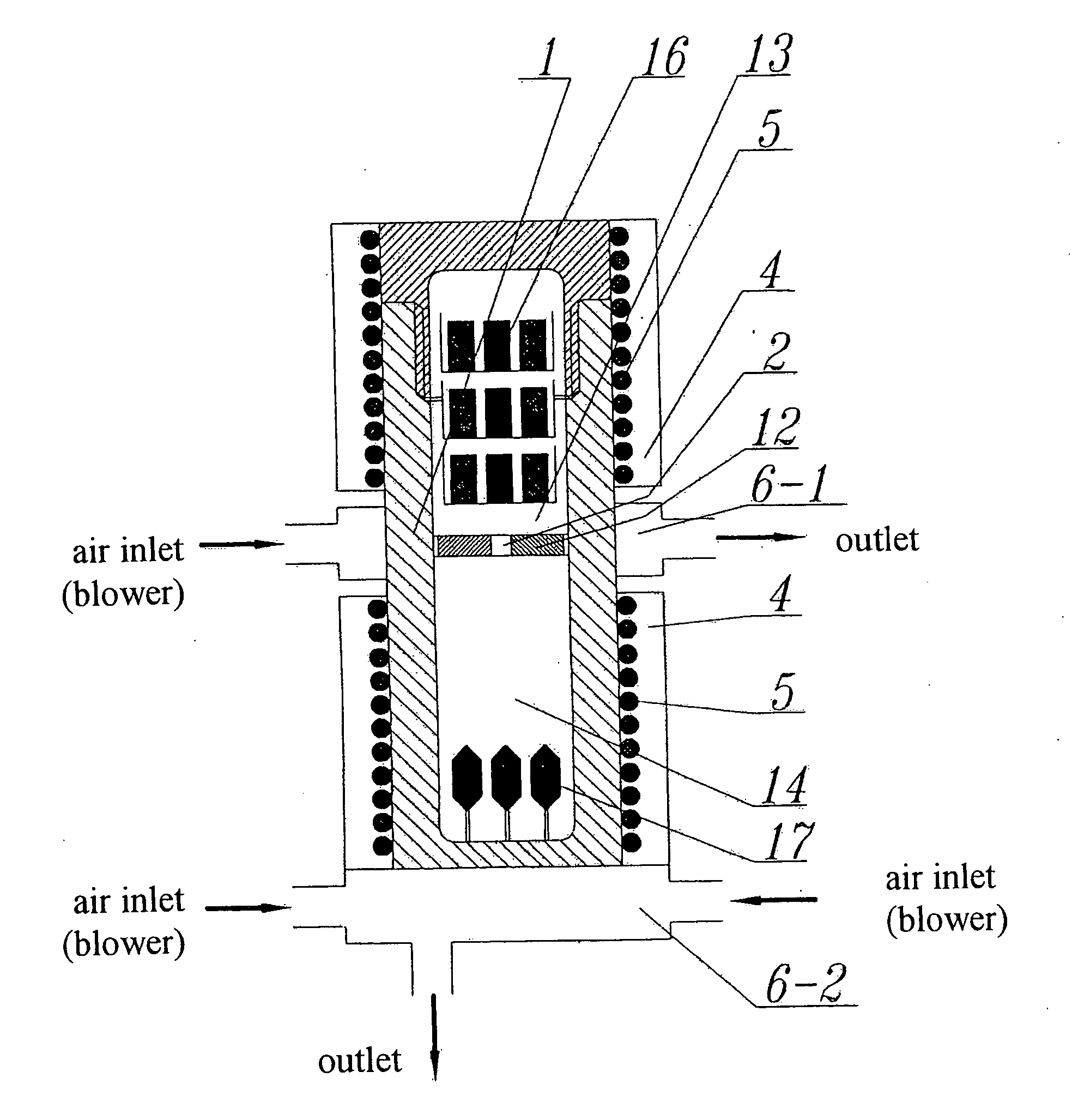
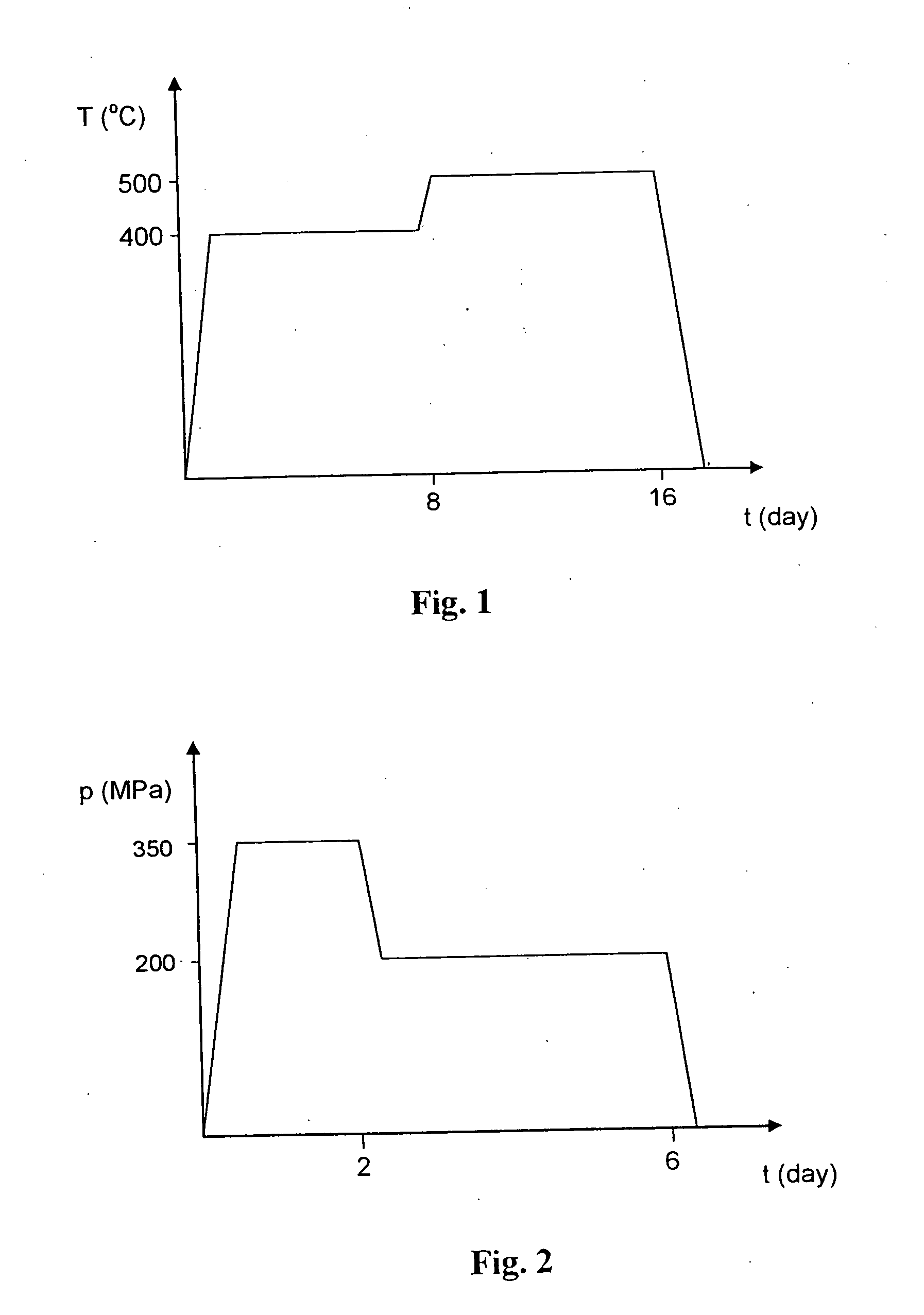
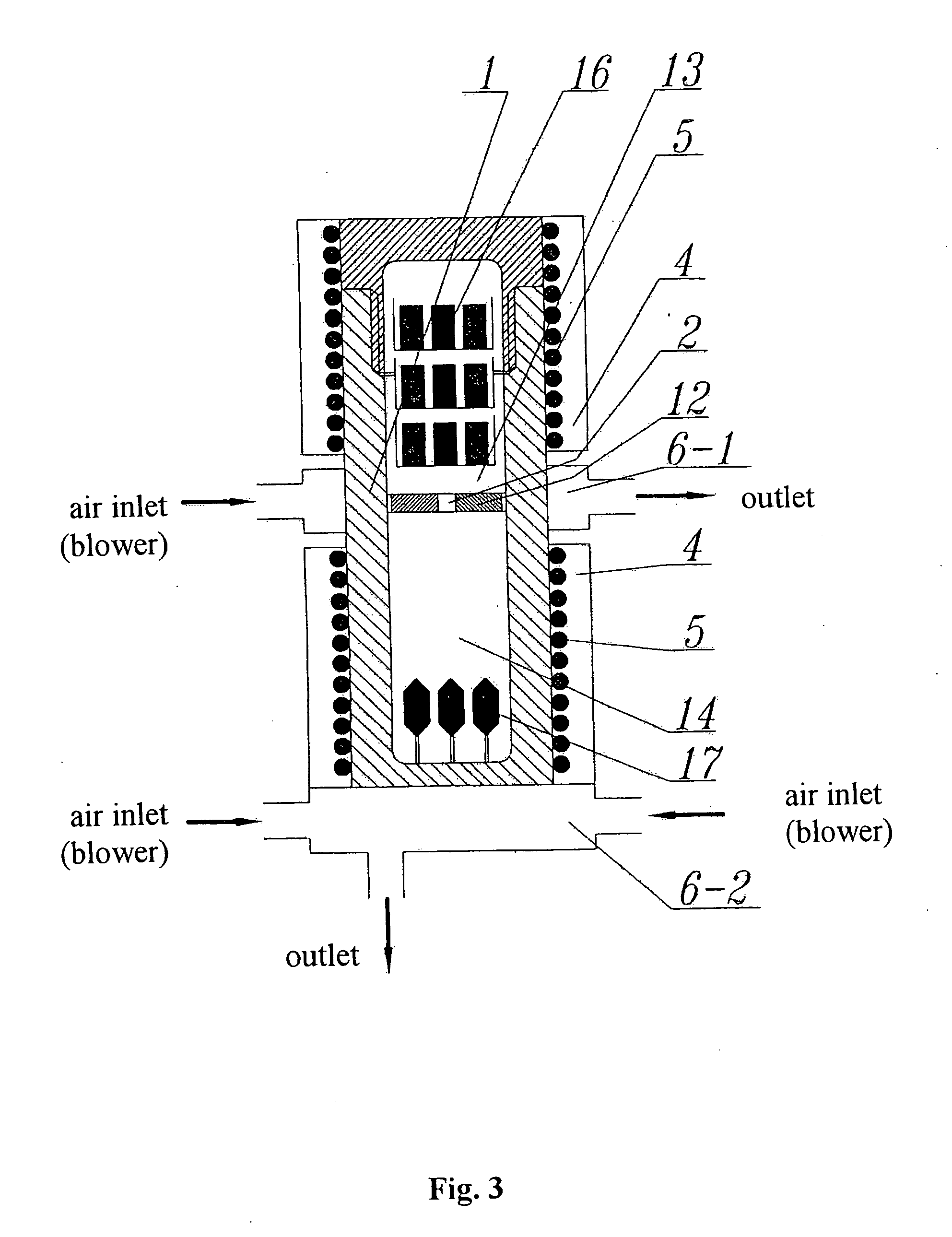
[0088] The dissolution zone 13 of a 600 cm3 high pressure autoclave 1, having the inner diameter of 40 mm and length of 480 mm, was charged with 53.0 g of feedstock in the form of metallic gallium (6N). The crystallization zone 14 of the same autoclave was charged with a seed crystal in the form of a gallium nitride wafer (having the diameter of about 1 inch and the mass of 2.0 g) obtained by means of A-axis direction growth in the supercritical ammono method as shown in FIG. 9. (the seed is made of the wafer having a length (L), an A-axis direction growth (W) from both sides of A-plane and edge periphery of M-planes) As the mineralizer, 12.0 g of 4N metallic sodium as well as 19.5 g of 4N metallic potassium were put into the autoclave. Next, the autoclave was filled with 255.0 g of ammonia (5N), tightly closed and put into a set of furnaces 4. The temperature of the dissolution zone 13 was raised to 450° C. (at 1° C. / min, FIG. 6), while the crystallization zone was not heated and i...


PUM


Abstract

The substrate is used for opto-electric or electrical devices and comprises a layer of nitride grown by means of vapor phase epitaxy growth wherein both main surfaces of the nitride substrate are substantially consisting of non N-polar face and N-polar face respectively and the dislocation density of the substrate is 5×10⁵/cm2 or less. Therefore, the template type substrate has a good dislocation density and a good value of FWHM of the X-ray rocking curve from (0002) plane less than 80, so that the resulting template type substrate is very useful for the epitaxy substrate from gaseous phase such as MOCVD, MBE and HVPE, resulting in possibility of making good opto-electric devices such as Laser Diode and large-output LED and good electric devices such as MOSFET.

Description

TECHNICAL FIELD [0001] This invention is related to a substrate for epitaxy used to make opto-electric devices such as LED and LD or electric devices such as MOSFET. BACKGROUND ART [0002] The currently used substrates for a vapor phase epitaxy typically include Sapphire, SiC, GaAs and Si and the resulting epitaxy layers grown on the substrate have been still in the unfavorably high dislocation density of 109 / cm2. Therefore, there have been proposed an application of ELOG-type structures to the substrate, which allows to decrease the dislocation density down to 106 / cm2, but that density is still too high to ensure the correct functioning of many electronic and opto-electronic devices, particularly high power semiconductor lasers. Further, there is another problem that the resulting substrates have a decreased epitaxy face area because of the ELOG structure. Accordingly, we have proposed the other processes for obtaining mono-crystalline gallium-containing nitrides, For example, Polis...

Claims


Application Information

Patent Timeline
IPC IPC(8): H01L21/322C30B15/14C30B25/02C30B25/18H01L21/20H01L33/32
CPCC30B25/02Y10T428/266C30B29/403C30B29/406H01L21/02389H01L21/0245H01L21/02458H01L21/0254H01L21/0262H01L21/02516H01L21/02576H01L21/02579H01L21/02581H01L21/02628H01L21/02636C30B25/18H01L21/20
Inventor DWILINSKI, ROBERTDORADZINSKI, ROMANGARCZYNSKI, JERZYSIERZPUTOWSKI, LESZEKKANBARA, YASUO
Owner AMMONO SP Z O O (PL)
Why Eureka
Try Eureka