
Plasma treatment for purifying copper or nickel

Inactive Publication Date: 2006-03-16
KOLEKTOR GRP D O O
View PDF25 Cites 195 Cited by
  • Summary
  • Abstract
  • Description
  • Claims
  • Application Information

AI Technical Summary

Benefits of technology

[0015] A special aspect of the present invention is to be seen in the fact that, by virtue of the specific conditions during the treatment, little or no bombardment of the surface with high-energy ions takes place, and this is regarded as particularly favorable.
[0016] The use of the inventive method for treatment of electronic components that are made from copper or nickel or that are coated therewith leads to several distinct advantages. It permits good adhesion of any material deposited on the surface, including cement, dye and low-temperature soldering metal, it ensures good electrical conductivity by the contact area of component and coating, it is ecologically favorable, and its operating costs and maintenance are minimal. In this regard the invention exploits the knowledge that plasma machining, by reducing the concentration of impurities at the surface of the components, increases the adhesion of the adjacent layer and lowers the electrical resistance by the connection area.
[0017] The surface plasma-treated according to the invention is passivated, which leads to longer resistance to corrosion by air or water. In addition, such a surface permits very good adhesion of any material deposited on the surface, including cement, dye and soldering metal.

Problems solved by technology

None of these methods, however, ensures perfect cleanness of the components.
However, copper is very susceptible to oxidation.
In the case of deposited copper layers, oxidation is viewed as a disadvantage, and it interferes with adhesion to the adjacent layer, impairs the conductivity of the copper structural element and reduces the reliability of the entire circuit.

Method used


Image

  • Plasma treatment for purifying copper or nickel
  • Plasma treatment for purifying copper or nickel
  • Plasma treatment for purifying copper or nickel

Examples


Embodiment Construction

OF THE INVENTION

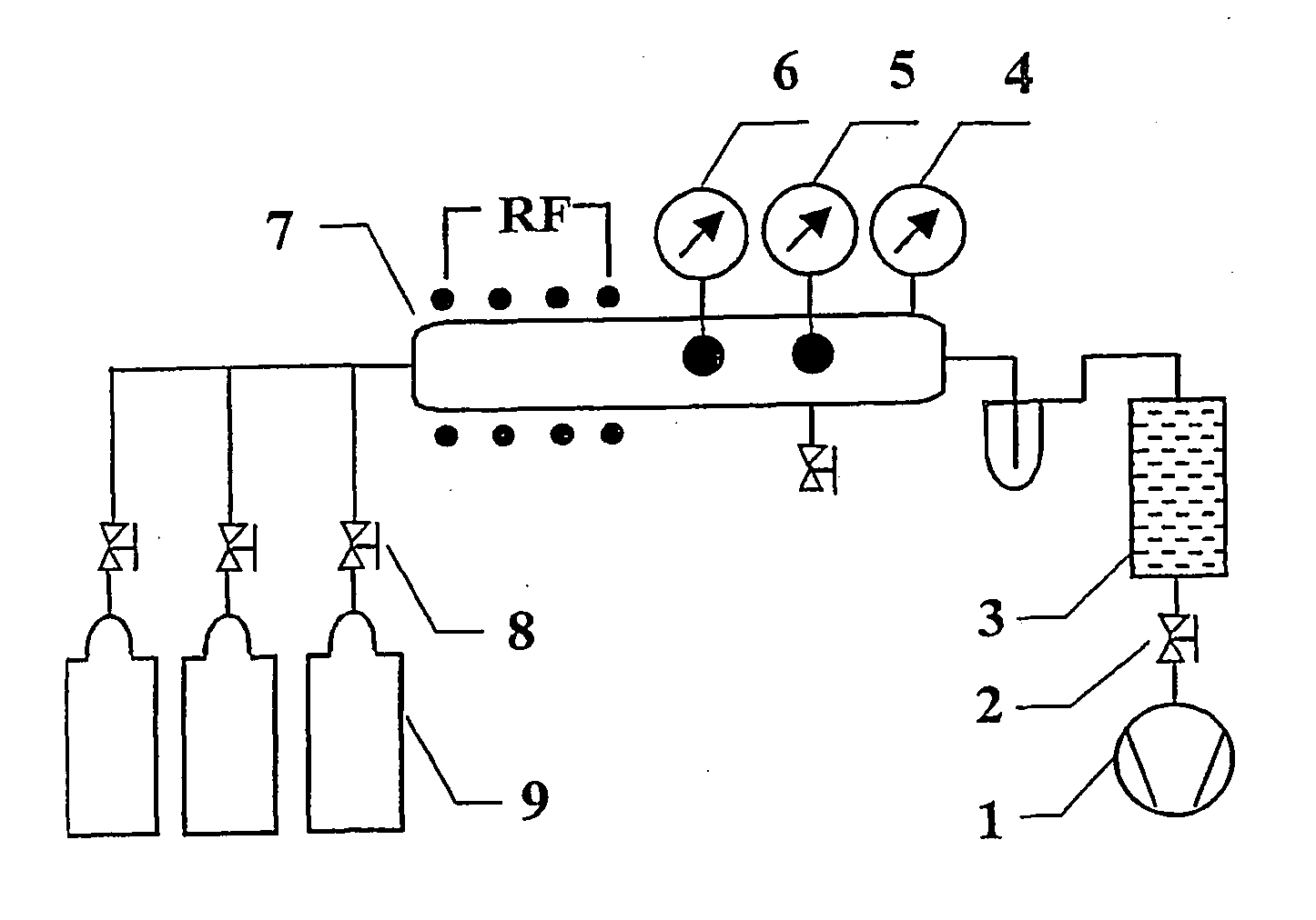
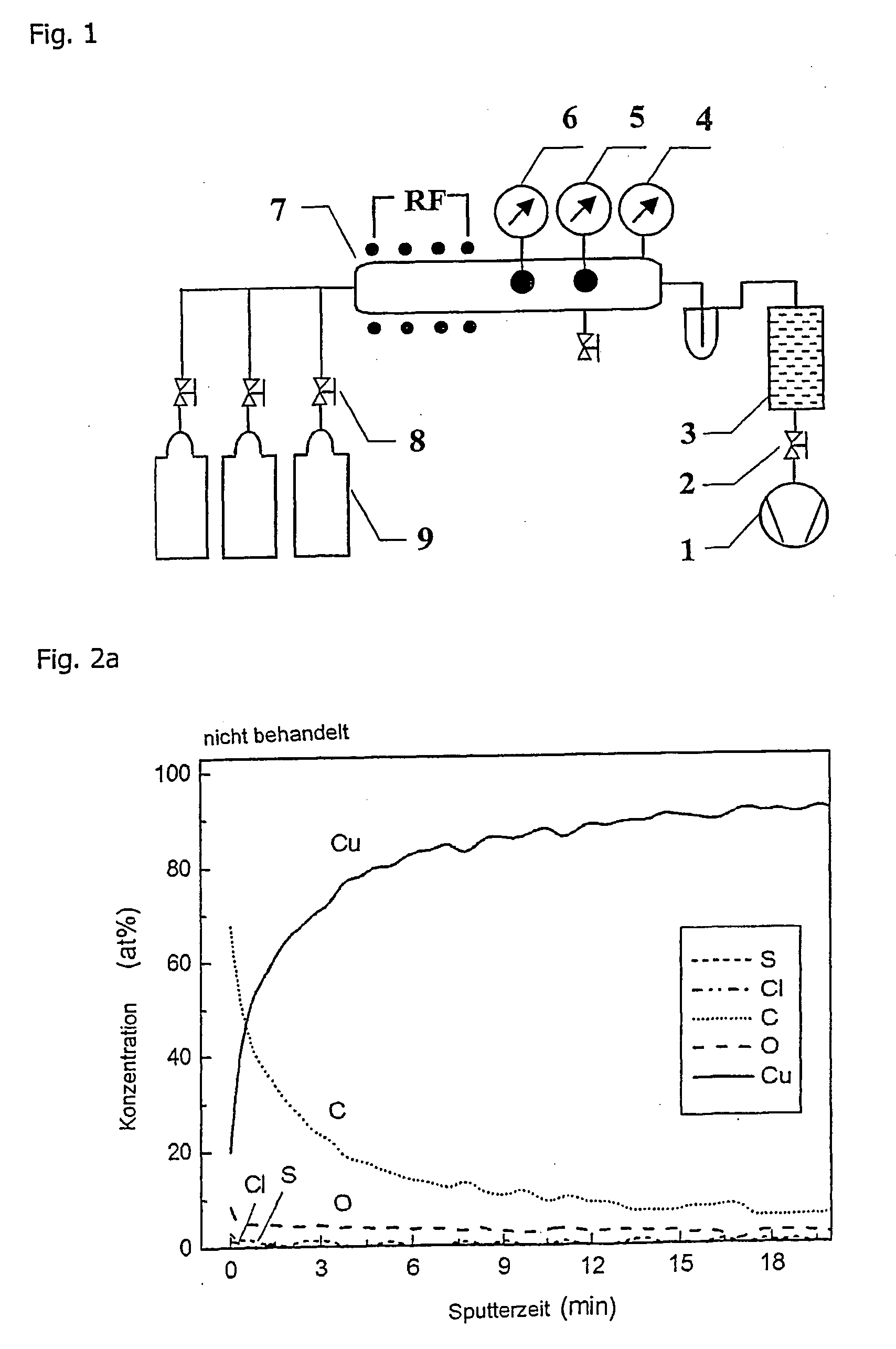
[0023] An example of a system configuration for plasma treatment of copper or nickel is shown in the schematic diagram of FIG. 1. The system is composed of a discharge chamber 7, a vacuum pump 1 having a valve 2, a trap vessel 3 containing sieves, three different outlet valves 8 and three gas bottles 9—oxygen, hydrogen and another gas (especially noble gas), and it achieves effective and economic treatment. The plasma parameters during the etching operation, such as the dose of radicals in the discharge chamber, are controlled by a vacuum gauge 4 and two or more sensors, such as catalytic sensor 5 and Langmuir sensor 6. The flux of radicals is adjusted to greater than approximately 1021, preferably greater than 1022 or, even more favorably, greater than 1024 radicals per square meter per second.

[0024] The rate at which the radicals are formed in the gaseous plasma containing an oxidizing gas (preferably oxygen or water vapor) depends on the power of the discharge so...


PUM

PropertyMeasurementUnit
Pressureaaaaaaaaaa
Pressureaaaaaaaaaa
Pressureaaaaaaaaaa

Abstract

A method for treating electronic components made of copper, nickel or alloys thereof or with materials such as brass or plated therewith and includes the steps of arranging the components in a treatment chamber, generating a vacuum in the treatment chamber, introducing oxygen into the treatment chamber, providing a pressure ranging between 10−1 and 50 mbar in the treatment chamber and exciting a plasma in the chamber, allowing the oxygen radicals to act on the components, generating a vacuum in the treatment chamber, introducing hydrogen into the treatment chamber, providing a pressure ranging between 10−1 and 50 mbar in the treatment chamber and exciting a plasma in the chamber and allowing the hydrogen radicals to act on the components.

Description

CROSS-REFERENCE TO RELATED APPLICATION [0001] This application is a continuation of International Application PCT / EP2004 / 004904 filed on May 7, 2004, now International Publication Number WO 2004 / 098259 and claims priority from German Patent Application 103 20 472.5 filed May 8, 2003, the contents of which are herein wholly incorporated by reference. TECHNICAL FIELD [0002] The present invention relates to a treatment method, using reactive plasmas, especially for cleaning electronic components that are made of copper or nickel or of alloys thereof such as brass or that are coated therewith. BACKGROUND OF THE INVENTION [0003] Components that are made of copper or nickel or alloys thereof such as brass, or that are coated therewith, are typically covered with a layer of impurities. At least a native layer of oxide is always present on the surface. Quite often the components are also contaminated with various organic and inorganic impurities. Organic impurities are often residues of oil...

Claims


Application Information

Patent Timeline
IPC IPC(8): B08B6/00C23G1/00B08B7/00B23K1/20C23G5/00
CPCB08B7/0035C23G5/00B23K1/20H05K3/26B08B7/00
Inventor MOZETIC, MIRANCVELBAR, UROS
Owner KOLEKTOR GRP D O O
Learn More