Binary OPC for assist feature layout optimization

a feature layout and binary opc technology, applied in the field of photolithography, can solve problems such as catastrophic failures, and achieve the effects of preventing catastrophic failures, poor process window, and superior gate level process

Inactive Publication Date: 2006-03-16
IBM CORP
View PDF18 Cites 29 Cited by
  • Summary
  • Abstract
  • Description
  • Claims
  • Application Information

AI Technical Summary

Benefits of technology

[0037] Implemented in the rules-based OPC SRAF design flow, the effect of binary OPC is to widen critical feature edges to compensate for the under-biasing resulting from the shortcomings of the one-dimensional SRAF rules table below. While this simple binary sort-and-widen approach of critical edge correction cannot promise to reproduce the original feature size accurately, it prevents catastrophic failures due to feature pinching. Binary OPC still has utility when using model-based OPC. Even though in model-based OPC, the line width at best focus will be corrected, the limited Depth of Focus (DOF) of an unassisted line can cause catastrophic failures. Thus, binary OPC in conjunction with optimized SRAF style options, yields a superior gate level process whether rule-based or modelOPC is used.
[0038] Thus there is a need for a solution to that problem which is provided by the present invention which provides a way to find edge segments of primary features that should have SRAF features which are missing, to bias the primary features so that they print large (although with poor process window) rather than small and with poor process window. Thus, the present invention (binary OPC) makes the pattern a little more robust, since small and poor quality edge segments have a tendency to break. Two ways of biasing these primary edge segments: 1) go in and “push the edge out”; i.e. move the edge out by a certain amount; or 2) provide the model-based OPC tool with a target pattern having a target edge pushed out to indicate that the line to be printed is wider thereby causing the model-based OPC tool to move the edge in the desired direction to produce a suitable result. The benefit of this process of causing the model based OPC to widen the line by pushing the edge to widen the image is that the model-based OPC tool keeps track of all the surrounding features and will help prevent turning one problem (a small / narrow and poor quality line) into a new problem which would result in features that are too wide and / or and merged with neighboring features. Glossary
[0046] Model-based OPC=feature selective biasing of the mask patterns to compensate for systematic patterning errors based on iterative movement of feature edges to reduce the difference between a simulated contour that is calculated using a calibrated process model and the desired wafer pattern, also known as the target pattern. In most cases, the target pattern is identical to the circuit layout.

Problems solved by technology

While this simple binary sort-and-widen approach of critical edge correction cannot promise to reproduce the original feature size accurately, it prevents catastrophic failures due to feature pinching.
Even though in model-based OPC, the line width at best focus will be corrected, the limited Depth of Focus (DOF) of an unassisted line can cause catastrophic failures.

Method used


Image

  • Binary OPC for assist feature layout optimization
  • Binary OPC for assist feature layout optimization
  • Binary OPC for assist feature layout optimization

Examples


first embodiment

of the Invention

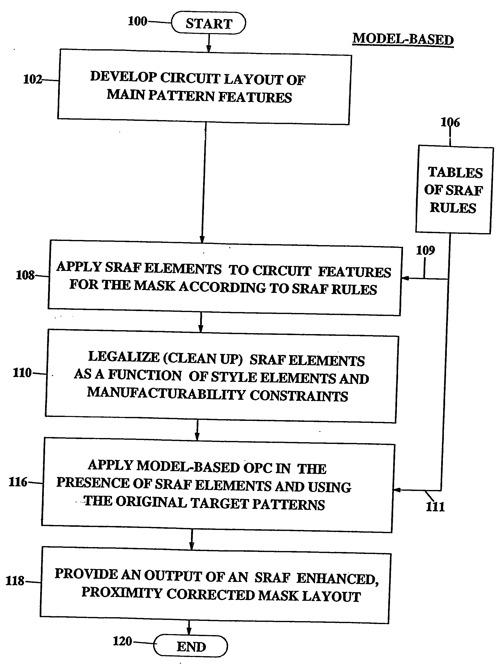
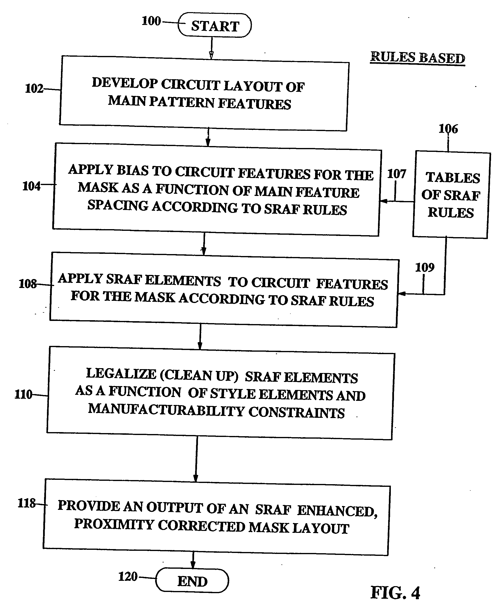
Rules-Based Binary-Optical Proximity Correction (OPC) with SRAF

[0120]FIG. 8 is a flow chart illustrating an application of Binary OPC steps to the Rules-Based SRAF elements, which incorporates main feature sizing as part of the SRAF design, which is a modification of the flow chart of FIG. 4, with the addition of steps 112 and 114. As in FIGS. 4 and 5, the program START begins with step 100 which leads to step 102. In step 102, the first data processing system develops a circuit layout of main pattern features of a chip that are input into the CAD system that includes a data entry unit such as a keyboard, a CPU and a DSD, inter alia. The steps 102, 104, 108 and 110 as well as rules table 106, are identical to those described above in connection with the Rules Based SRAF process described with reference to FIG. 4.

[0121] The first new step of the method of this invention is step 112 in which the system identifies problem (critical) edge segments of a main pattern fe...

second embodiment

of the Invention

Model-Based Optical Proximity Correction (OPC) with SRAF

[0125]FIG. 9 is a flow chart illustrating a Binary OPC implementation in the Model-Based SRAF elements flow chart of FIG. 5. In FIG. 9 a modified step 114′ based on the selective bias step 114 of FIG. 8 is applied to the Model-Based SRAF flow chart of FIG. 5. As in FIGS. 4, 5 and 8, the START step 100 leads to step 102. The steps 102, 108 and 110 as well as the table of SRAF rules 106, are the same as in FIG. 5 and step 112 which is the same as in FIG. 8 follows step 110 as in FIGS. 5 and 8. The process of FIG. 9 omits the step 104 of FIGS. 4 / 8 and performs the step 108 in place thereof.

[0126] In step 112, the CAD system must apply rules to identify the problem edge segments of the main pattern features based upon insufficient SRAF element coverage, i.e. which SRAF elements of the current design of the mask being developed by the CAD system are at risk of being spaced too far apart and therefore require perfo...


PUM

PropertyMeasurementUnit
sizeaaaaaaaaaa
pressureaaaaaaaaaa
physicalaaaaaaaaaa

Abstract

A method of forming a photolithographic mask layout with Sub-Resolution Assist Feature (SRAF) elements on a mask for correcting for proximity effects for a pattern imaged comprising the steps of developing a layout of mask features for printing main pattern features. Provide a table of SRAF element data including spacing of main pattern features and SRAF elements, applying SRAF elements to the mask layout as a function of spacing of main pattern features and SRAF elements, legalizing the SRAF elements as a function of style options, and providing a target pattern comprising a modified layout for the mask, identifying problem edge segments of an SRAF element of the target pattern at risk of causing a printing defect, applying a selected bias to the problem edge segments to modify the pattern where there are areas of SRAF element loss, and providing an output of a modified pattern with modified SRAF elements removing the areas of SRAF element loss. The system can provide SRAF elements to the mask layout as a function of spacing of main pattern features and SRAF elements may be based on data from the SRAF table; or the system can applying model based OPC for exposure dose values based on data from the SRAF table.

Description

BACKGROUND OF THE INVENTION [0001] 1. Field of the Invention [0002] This invention relates to photolithography and more particularly to proximity correction in the presence of subresolution assist features used in photolithography. [0003] 2. Description of Related Art [0004] A very large scale integrated (VLSI) complementary metal oxide semiconductor (CMOS) chip is manufactured on a silicon wafer by a sequence of material additions (i.e., low pressure chemical vapor depositions, sputtering operations, etc.), material removals (i.e., wet etches, reactive ion etches, etc.), and material modifications (i.e., oxidations, ion implants, etc.). These physical and chemical operations interact with the entire wafer. For example, if a wafer is placed into an acid bath, the entire surface of the wafer will be etched away. In order to build very small electrically active devices on the wafer, the impact of these operations has to be confined to small, well defined regions. [0005] Lithography in...

Claims


Application Information

Patent Timeline
Patent Type & Authority Applications(United States)
IPC IPC(8): G03C5/00G03F1/00G03F1/36G03F9/00G06F17/50
CPCG03F1/36G03F1/144
Inventor LIEBMANN, LARS W.FERGUSON, RICHARD A.GABOR, ALLEN H.LAVIN, MARK A.
Owner IBM CORP
Why Eureka
Try Eureka