Light emitting diode structures
a technology of light-emitting diodes and structures, which is applied in the direction of instruments, optical elements, optical waveguide light guides, etc., can solve the problems of reducing the efficiency of light extraction, so as to improve the extraction efficiency, and improve the effect of mode confinemen
- Summary
- Abstract
- Description
- Claims
- Application Information
AI Technical Summary
Benefits of technology
Problems solved by technology
Method used
Image
Examples
Embodiment Construction
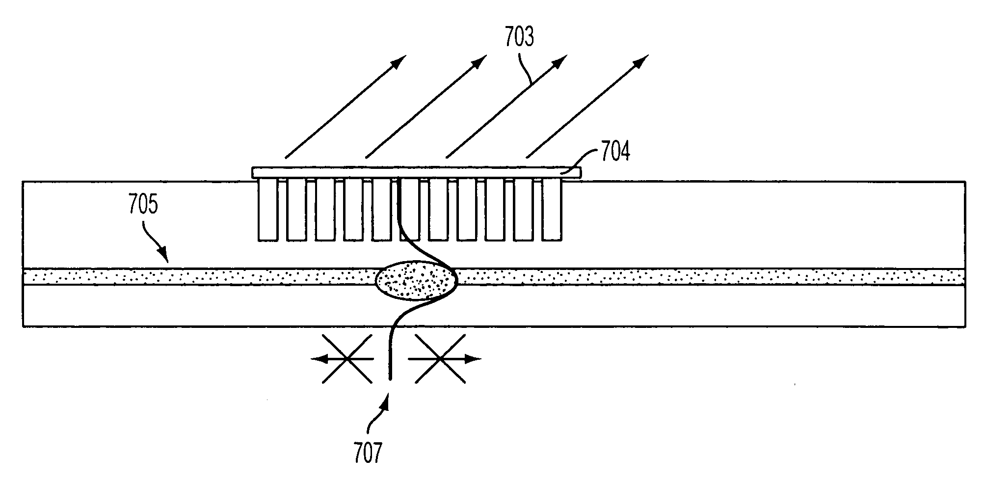
[0059] There are three possible uniform tilings of the plane by regular polygons, using squares, triangles or hexagons. In 1-uniform tilings there is only one type of vertex in the plane. Additionally there are 13 different orientations for filling the space using 1-uniform (Archimedian) tilings. These tiling patterns form the basis of what, in this specification, will be referred to as regular 2D photonic crystals. Regular 2D photonic crystals are typically formed in dielectric material and have an array of regions forming a periodic variation in refractive index, the periodicity based on one of the uniform tilings of the plane. The simplest example of a photonic crystal of this type is an array of holes in a dielectric slab, an etched air rod being positioned at each vertex of a uniform tiling pattern.
[0060] Photonic crystals offer unique ways to tailor light and the propagation of electromagnetic (EM) waves. By analogy to electrons in a crystal, EM waves propagating in a structu...
PUM
 Abstract
Description
Claims
Application Information


