Leak detector and process gas monitor

a technology of gas monitor and leak detector, which is applied in the direction of energy-based chemical/physical/physicochemical processes, transportation and packaging, and nuclear engineering, etc., can solve the problems of leakage of gas monitors, damage to particular devices on the substrate, and contamination of substrates falling on the substrates

Inactive Publication Date: 2006-04-13
APPLIED MATERIALS INC
View PDF33 Cites 20 Cited by
  • Summary
  • Abstract
  • Description
  • Claims
  • Application Information

AI Technical Summary

Benefits of technology

[0012] The present invention generally provides a method and apparatus for a plasma enhanced chemical vapor deposition system for processing one or more flat panel display substrates comprising a vacuum deposition process chamber configured to contain gas, a residual gas analyzer configured to analyze the gas within the process chamber and to provide feedback, and a controller to monitor feedback from the gas analyzer. Also, the present invent

Problems solved by technology

During subsequent depositions, the film on the chamber surfaces can crack or peel, causing contaminants to fall on the substrate.
This causes problems and damage to particular devices on the substrate.
If the pressure rise is not within an expected range, the chamber may be experiencing a leak.
The leak may be from a faulty seal in a process gas valve.
Alternatively, it may be a leak across any of the O-ri

Method used


Image

  • Leak detector and process gas monitor
  • Leak detector and process gas monitor
  • Leak detector and process gas monitor

Examples


Embodiment Construction

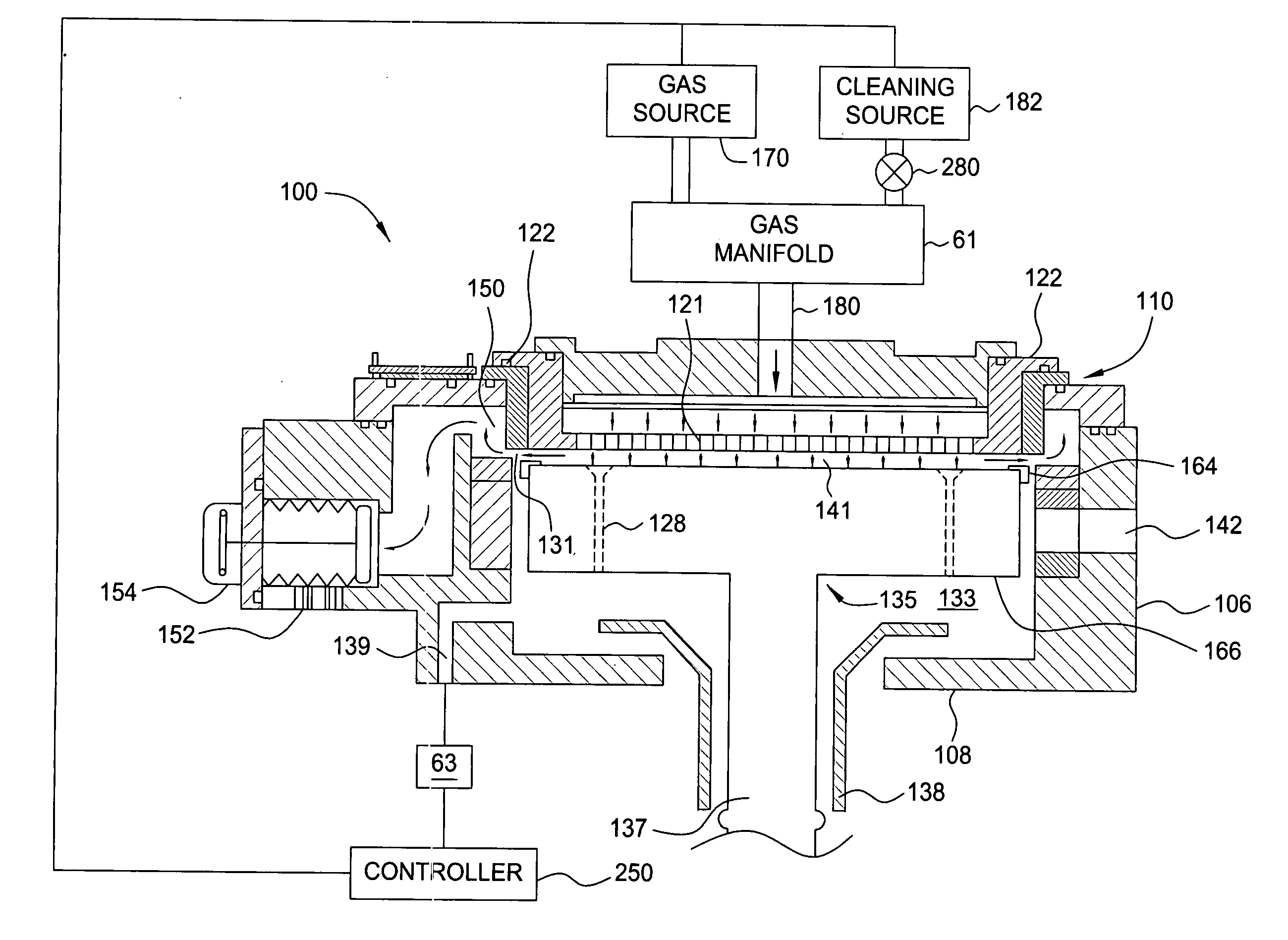
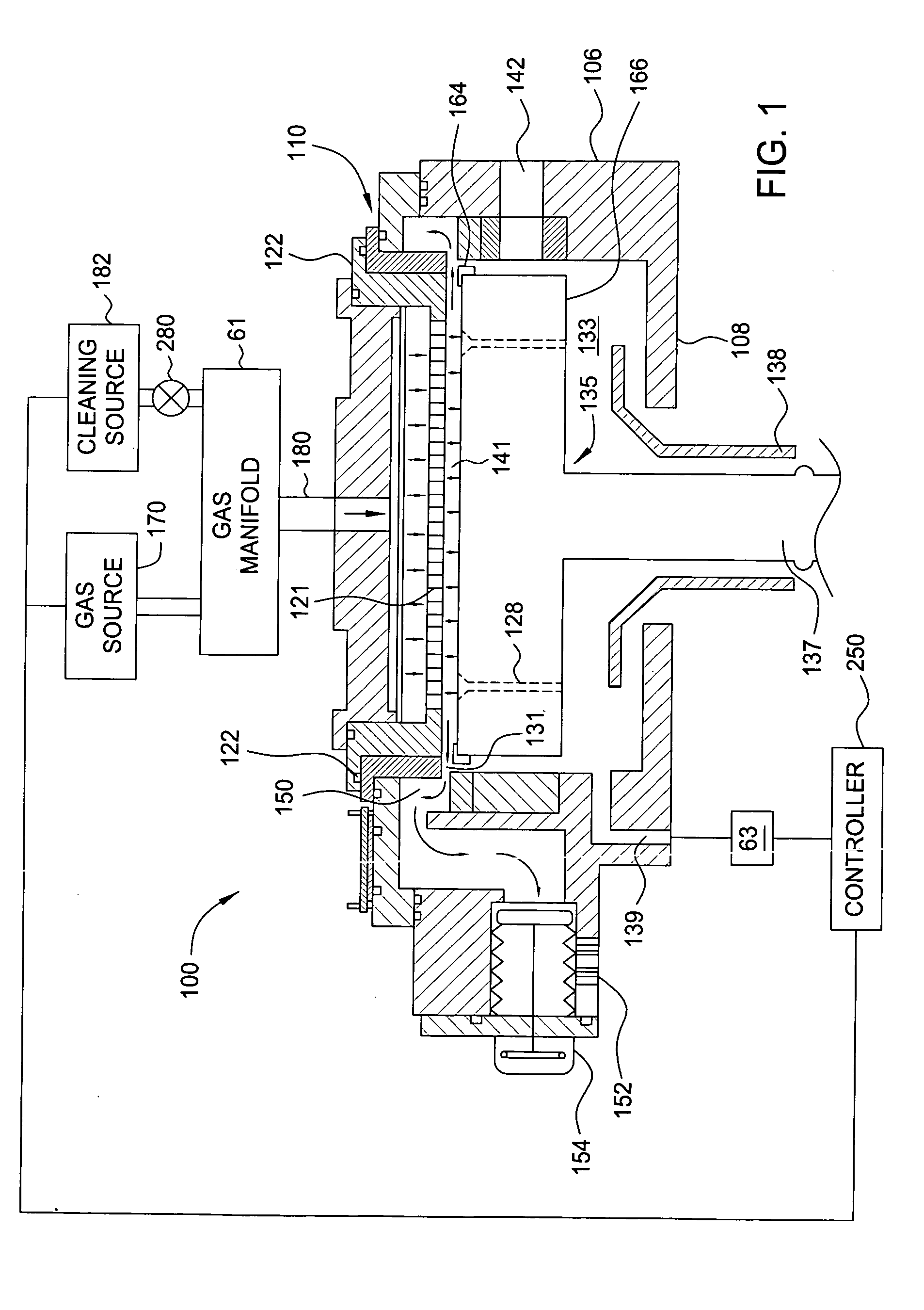
[0016]FIG. 1 illustrates a schematic cross-sectional view of one embodiment of a plasma enhanced chemical vapor deposition (PECVD) system 100, which is available from AKT, a division of Applied Materials, Inc., of Santa Clara, Calif. The system 100 includes a vacuum deposition process chamber 133. The process chamber 133 has walls 106 and a bottom 108 that partially define a processing region 141. The walls 106 and the bottom 108 are typically fabricated from a unitary block of aluminum or other material compatible with processing. The walls 106 have an opening 142 for transferring flat panel display substrates into and out of the process chamber 133. Examples of flat panel display substrates include glass substrates, polymer substrates, and the like. Although various embodiments of the invention are described with reference to PECVD systems, other embodiments of the invention may apply to cluster process systems, in-line systems, stand-alone systems and the like.

[0017] A temperatu...


PUM

PropertyMeasurementUnit
Partial pressureaaaaaaaaaa
Flow rateaaaaaaaaaa

Abstract

A method and apparatus for a plasma enhanced chemical vapor deposition system for processing one or more flat panel display substrates comprising a vacuum deposition process chamber configured to contain gas, a residual gas analyzer configured to analyze the gas within the process chamber and to provide feedback, and a controller to monitor feedback from the gas analyzer. Also, a method for identifying a process upset within a plasma enhanced chemical vapor deposition system configured to process flat panel display substrates comprising determining a historical slope of a line for partial pressure as a function of time, calculating a new slope of a line based on partial pressure measurements by a residual gas analyzer, comparing the historical and new slopes, and sending a signal to an operator.

Description

CROSS-REFERENCE TO RELATED APPLICATIONS [0001] This application claims benefit of U.S. provisional patent application Ser. No. 60 / 617,714, filed Oct. 12, 2004, which is herein incorporated by reference.BACKGROUND OF THE INVENTION [0002] 1. Field of the Invention [0003] Embodiments of the present invention generally relate to flat panel display and semiconductor wafer processing and methods, and more particularly, to methods and systems for monitoring the status of flat panel display processing systems. [0004] 2. Description of the Related Art [0005] Chemical vapor deposition (CVD) is widely used in the semiconductor industry to deposit films such as intrinsic and doped amorphous silicon (a-Si), silicon oxide (SixOy), silicon nitride (SirNs), and silicon oxynitride, on a substrate. Modern semiconductor CVD processing is generally done in a vacuum chamber by using precursor gases which dissociate and react to form the desired film. In order to deposit films at low temperatures and rel...

Claims


Application Information

Patent Timeline
IPC IPC(8): C23C16/00C23F1/00H01L21/306B01J19/08
CPCC23C16/4401C23C16/52H01J37/32935H01J37/3299H01L21/67253
Inventor LEUNG, SAMUELBONNE, ULRICH A.
Owner APPLIED MATERIALS INC
Why Eureka
Try Eureka