Method of detecting etching end-point

Inactive Publication Date: 2006-05-18
SAMSUNG ELECTRONICS CO LTD
View PDF1 Cites 4 Cited by
  • Summary
  • Abstract
  • Description
  • Claims
  • Application Information

AI Technical Summary

Problems solved by technology

In the active layer etching process, since an etching speed is not fixed and an interface state between the clad (or active layer) and the mask is not uniform, the width of the remaining active layer obtained through the etching process is not uniform even if the same mask is used.
However, when the width of the remaining active layer is observed through an optical microscope using a visible ray, it is difficult to exactly know the width of the remaining active layer as it is difficult to distinguish a difference of below 0.2 μm.
As described above, the conventional method of detecting an etching end-point using an optical microscope is not accurate.

Method used


Image

  • Method of detecting etching end-point
  • Method of detecting etching end-point
  • Method of detecting etching end-point

Examples


first embodiment

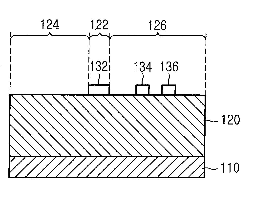
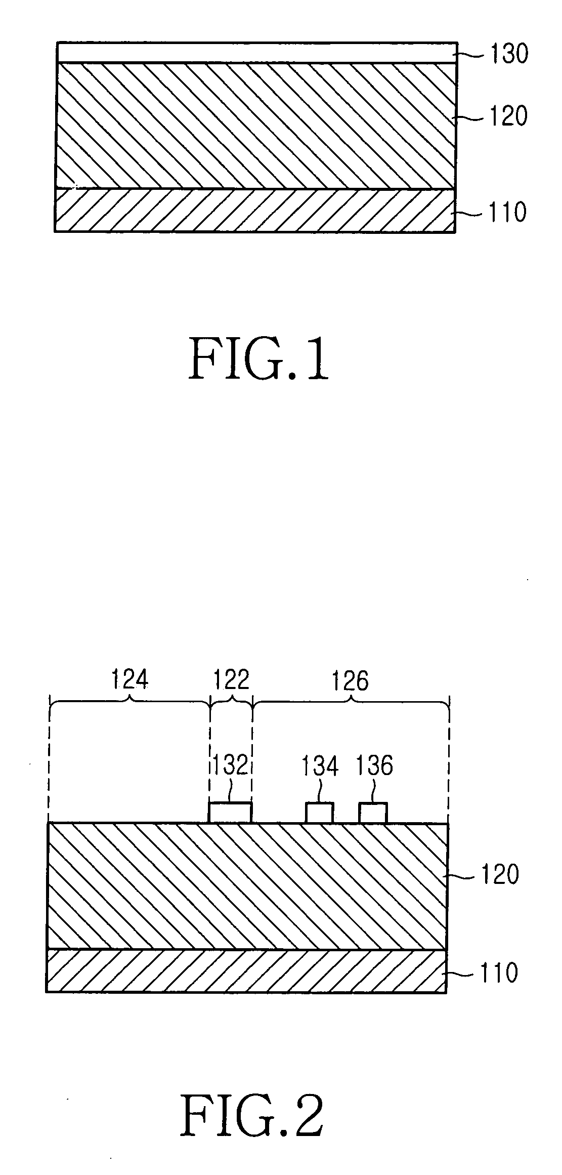
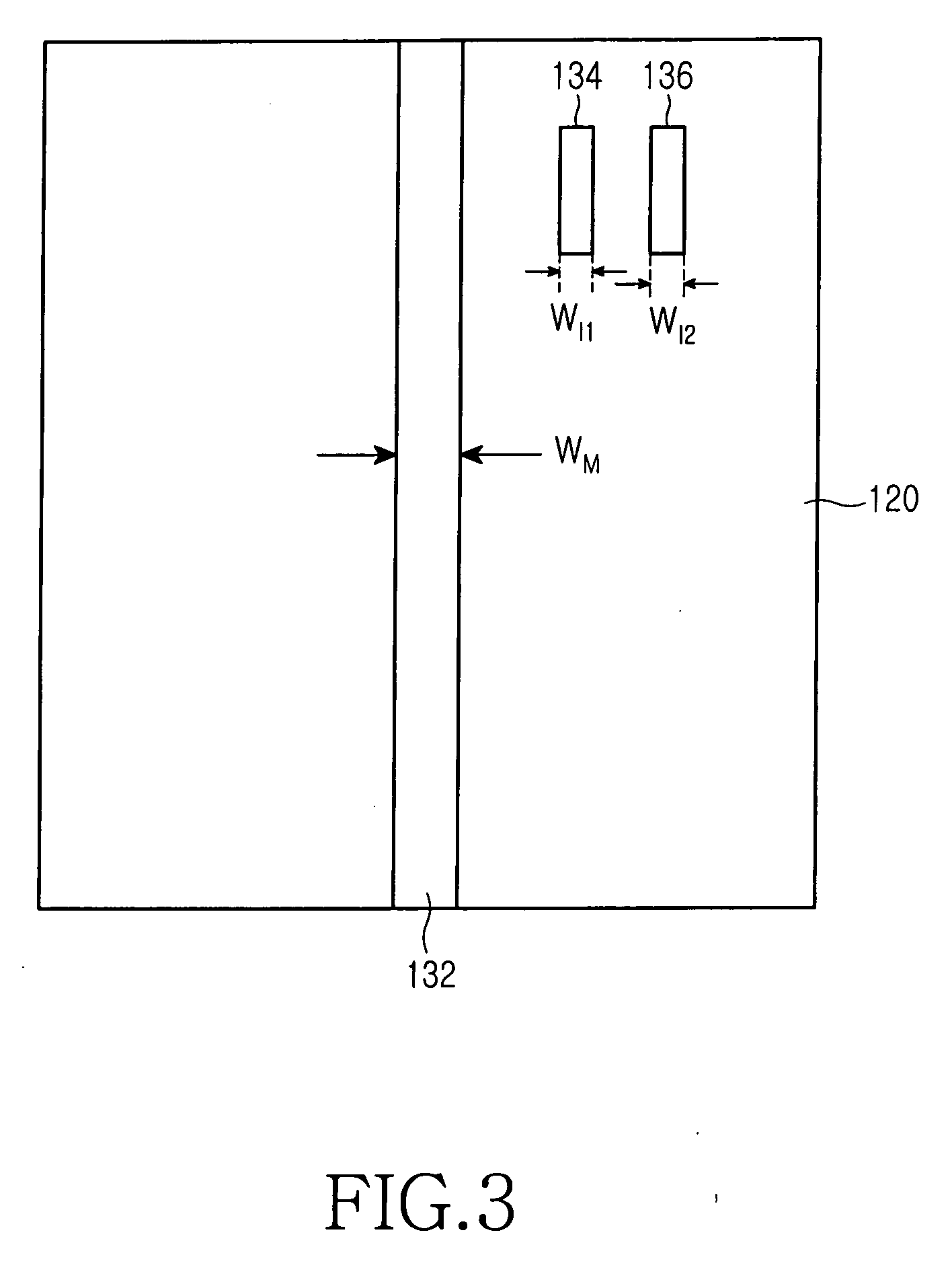
[0017] FIGS. 1 to 5 are diagrams illustrating a method of detecting an etching end-point chip by chip according to the present invention. In particular, FIGS. 1 to 3 are illustrative diagrams of forming etching indicators. Briefly, the method of detecting an etching end-point includes the steps of: forming etching indicators; and detecting the etching end-point using the etching indicators.

[0018] Referring to FIG. 1, an active layer 120 of a multi-quantum well (MQW) structure, which is an etching object, is grown on a chip-by-chip semiconductor substrate 110 using a metal-organic chemical vapor deposition (MOCVD) technique or a molecular beam epitaxy (MBE) technique. A photoresist photolithography is performed on the mask layer 130. A mask layer 130 of a dielectric substance such as SiO2 or SiNx is layered on the active layer 120. In addition to the dielectric substance, metal, a high molecular substance, or a substance such as a semiconductor having a different physical property fr...

second embodiment

[0035] FIGS. 8 to 10 are illustrative diagrams showing a method of detecting an etching end-point according to the present invention. Briefly, the method of detecting an etching end-point includes the steps of: forming etching indicators; and detecting the etching end-point using the etching indicators.

[0036]FIG. 8 is a diagram of a wafer 210 having first to seventh etching indicators 220 to 280. As shown, each of the first to seventh etching indicators 220 to 280 has an area of 1×1 mm, and the first to seventh etching indicators 220 to 280 are comprised of units 225 to 285 of a 100×70 matrix structure. The first to seventh etching indicators 220 to 280 have units of widths of 4.3 μm, 4.4 μm, 4.5 μm, 4.6 μm, 4.7 μm, 4.7 μm, and 4.9 μm in order. If necessary, a difference of the unit widths can be set to 0.01 to 2 μm. An active layer 214, which is an etching object, is formed on the wafer 210 divided into a plurality of chips 212. A rectangular mask 216 is formed in a pattern area of...


PUM

PropertyMeasurementUnit
Sizeaaaaaaaaaa
Widthaaaaaaaaaa
Sizeaaaaaaaaaa

Abstract

A method of detecting an etching end-point includes the steps of: forming a mask on a pattern area of an etching object; forming an etching indicator on an etching area of the etching object, which is not covered by the mask; etching the etching object using the mask; and evaluating the size of a remaining object covered by the mask using the etching indicator.

Description

CLAIM OF PRIORITY [0001] This application claims priority under 35 U.S.C. § 119 to an application entitled “Method of Detecting Etching End-Point,” filed in the Korean Intellectual Property Office on Nov. 17, 2004 and assigned Serial No. 2004-94374, the contents of which are incorporated herein by reference. BACKGROUND OF THE INVENTION [0002] 1. Field of the Invention [0003] The present invention relates generally to an etching process for fabricating semiconductor components and in particular, to a method of detecting an etching end-point during a process of etching objects to yield a desired pattern using a mask. More specifically, the present invention relates generally to a method of detecting an etching end-point at which the size of a remaining object covered by a mask reaches a target size. [0004] 2. Description of the Related Art [0005] A laser diode has an active layer with a narrow width in which a laser oscillates which is formed by growing a multi-quantum well (MQW) on a...

Claims


Application Information

Patent Timeline
IPC IPC(8): H01L21/76
CPCH01L22/20H01L22/34H01L21/306
Inventor KIM, YOUNG-HYUNBAE, YU-DONGLEE, JUNG-KEEKIM, IN
Owner SAMSUNG ELECTRONICS CO LTD
Why Eureka
Try Eureka