Semiconductor device, radiographic imaging apparatus, and method for manufacturing the same

a semiconductor device and radiographic imaging technology, applied in the direction of printed circuit repair/correction, dielectric characteristics, laminating printed circuit boards, etc., can solve the problem of difficult replacement of defective components

Inactive Publication Date: 2006-05-25
CANON KK
View PDF4 Cites 23 Cited by
  • Summary
  • Abstract
  • Description
  • Claims
  • Application Information

AI Technical Summary

Benefits of technology

[0008] Accordingly, the present invention provides a radiographic imaging apparatus in which the connection and the replacement of an electrical component can be perfor

Problems solved by technology

Thus, the replacement of a def

Method used


Image

  • Semiconductor device, radiographic imaging apparatus, and method for manufacturing the same
  • Semiconductor device, radiographic imaging apparatus, and method for manufacturing the same
  • Semiconductor device, radiographic imaging apparatus, and method for manufacturing the same

Examples


first embodiment

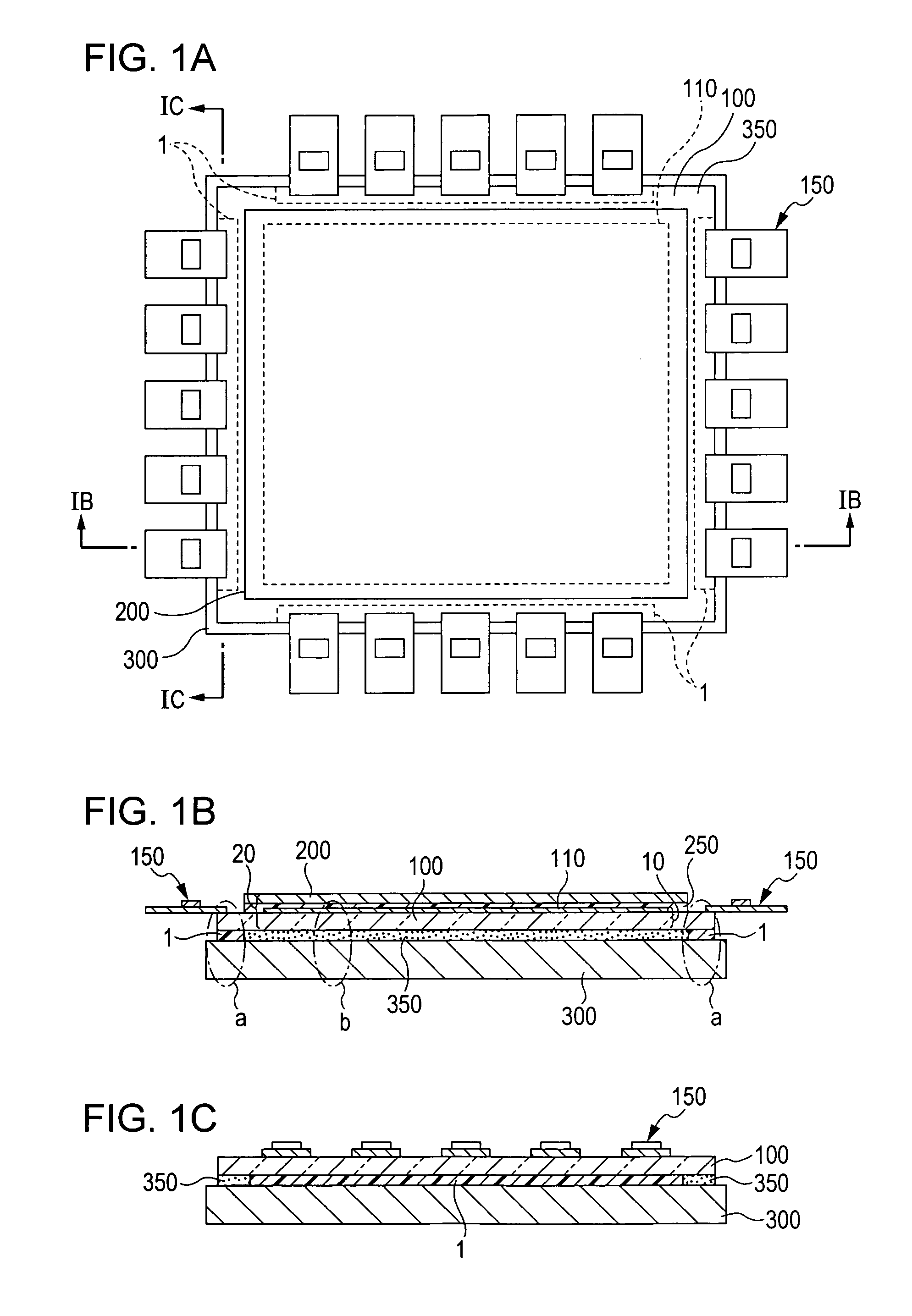
[0035]FIG. 1A is a schematic plan view of a radiographic imaging apparatus according to this embodiment; FIG. 1B is a schematic cross-sectional view taken along the line IB-IB of FIG. 1A; and FIG. 1C is a schematic cross-sectional view taken along the line IC-IC of FIG. 1A.

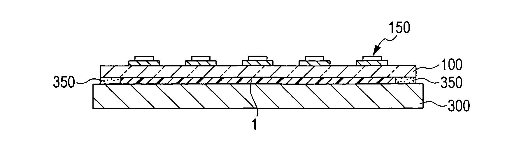
[0036] A pixel unit 110 is placed on a glass substrate 100. The pixel unit 110 includes pixels arranged in two dimensions. Each pixel is composed of a conversion element for converting radiation or light into electric signals and a signal transfer element, such as TFT. A drive wire for driving signal transfer means, a signal wire for reading the electric signals that have been converted in the conversion element and transferred by the signal transfer means, a bias wire for biasing the conversion element, and an electrical connection portion for connecting these wires to an external circuit are provided on the periphery of the pixel unit 110 on the substrate 100. The substrate 100, the pixel unit 110, the drive wi...

second embodiment

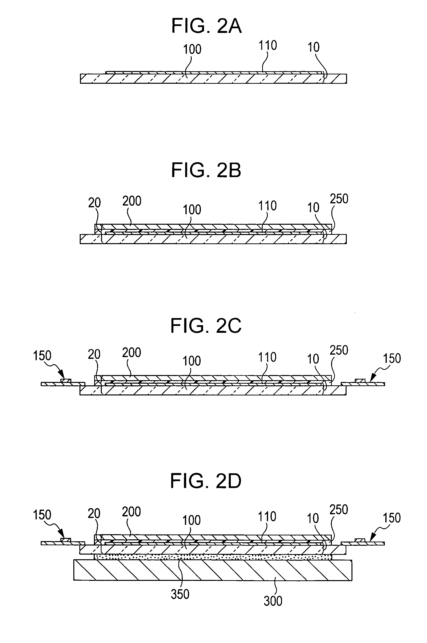
[0065]FIG. 4A to FIG. 4C are schematic views of a radiographic imaging apparatus according to a second embodiment. FIG. 4A is a schematic plan view of the radiographic imaging apparatus according to the second embodiment; FIG. 4B is a schematic cross-sectional view taken along the line IVB-IVB of FIG. 4A; and FIG. 4C is a schematic cross-sectional view taken along the line IVC-IVC of FIG. 4A. Like components are denoted by like numerals in the first embodiment and will be explained briefly or will not be further explained.

[0066] In the second embodiment, as in the first embodiment, a pixel unit 110, a drive wire, a signal wire, a bias wire, and an electrical connection portion are placed on a glass substrate 100. The substrate 100, the pixel unit 110, the drive wire, the signal wire, the bias wire, and the electrical connection portion constitute a sensor panel 10. Electrical components 150 of TCPs are connected to the electrical connection portion on the periphery of the substrate...

third embodiment

[0070] The application of the radiographic imaging apparatus according to the present invention to an X-ray diagnosis system will be described below with reference to FIG. 5.

[0071] X-rays 6060 generated by an X-ray tube 6050 pass through a chest 6062 of a patient 6061 and enter a radiographic imaging apparatus (image sensor) 6040 as shown in FIG. 3. The incident X-rays contain information on the interior of the body of the patient 6061. The incident X-rays cause a scintillator (phosphor layer) to emit light, which is photoelectrically converted by photoelectric conversion elements in a sensor panel into electrical information. This electrical information is converted into digital data, which are subjected to image processing in an image processor 6070, which serves as signal processing means, and is visualized on a display 6080, which serves as displaying means, in a control room.

[0072] The electrical information can also be transferred to a remote place with transmission means, s...


PUM


Abstract

A semiconductor device or a radiographic imaging apparatus includes a substrate and a supporting member, the substrate having a semiconductor element or a conversion element and being bonded to the supporting member with a laminating member. The semiconductor device or the radiographic imaging apparatus further includes at least one cushioning member in at least one space between the substrate and the supporting member at least in a region including an electrical connection portion connected to at least one electrical component. Thus, when a malfunction or a defect is found in the at least one electrical component, such as TCP, on the periphery of the substrate, the defective electrical component can easily be replaced.

Description

BACKGROUND OF THE INVENTION [0001] 1. Field of the Invention [0002] The present invention relates to a radiographic imaging apparatus that detects radiation as an electric signal. The radiographic imaging apparatus can be used in medical diagnostic equipment or nondestructive testing equipment. The term “radiation” as used herein includes electromagnetic waves, such as alpha rays, beta rays, and gamma rays, as well as X-rays. [0003] 2. Description of the Related Art [0004] In general, an X-ray film system that has a fluorescent screen containing an X-ray phosphor layer and is coated on both sides has conventionally been used in X-ray photography. Recently, digital radiographic imaging apparatuses that include an X-ray phosphor layer and a two-dimensional photodetector (sensor panel) have widely been studied, and various patents have been applied for in relation thereto. The digital radiographic imaging apparatuses have advantages in that they have excellent image characteristics, an...

Claims


Application Information

Patent Timeline
IPC IPC(8): H01L23/34
CPCH01L27/14618H01L27/14663H05K3/0058H05K3/225H05K3/361H05K2201/0133H01L2924/0002H05K2201/10681H05K2201/2036H01L2924/00
Inventor TAKEDA, SHINICHI
Owner CANON KK
Why Eureka
Try Eureka