Photoelectric conversion element, solar battery, and photo sensor

Inactive Publication Date: 2006-06-08
SEMICON ENERGY LAB CO LTD
View PDF33 Cites 41 Cited by
  • Summary
  • Abstract
  • Description
  • Claims
  • Application Information

AI Technical Summary

Benefits of technology

[0027] It is to be noted that a photoelectric conversion element and a solar battery having the photoelectric conversion element with high energy conversion efficiency can be provided by providing an amplifier circuit. The amplifier circuits are, for example, a circuit formed of an operational amplifier and a thin film transistor (hereinafter referred to as a TFT) and the like.
[0028] According to a photoelectric conversion element and a solar battery having the photoelectric conversion element of the invention, each of the inorganic compound and the organic compound of the charge generating layer becomes a charge separation state as a result of electron transfer caused by light irradiation of natural light, laser light, sunlight or the like with a particular wavelength. On the other hand, a charge transfer complex formed by mixing an inorganic compound and an organic compound is created following excitation by li

Problems solved by technology

However, the dye thin film solar battery is disadvantageous in that conversion efficiency from an optical energy into an electrical energy only exceeds 1% and that conversion efficiency is low.
The dye sensitization solar battery of which conversion efficiency from an optical energy into an electrical

Method used


Image

  • Photoelectric conversion element, solar battery, and photo sensor
  • Photoelectric conversion element, solar battery, and photo sensor
  • Photoelectric conversion element, solar battery, and photo sensor

Examples


embodiment mode 1

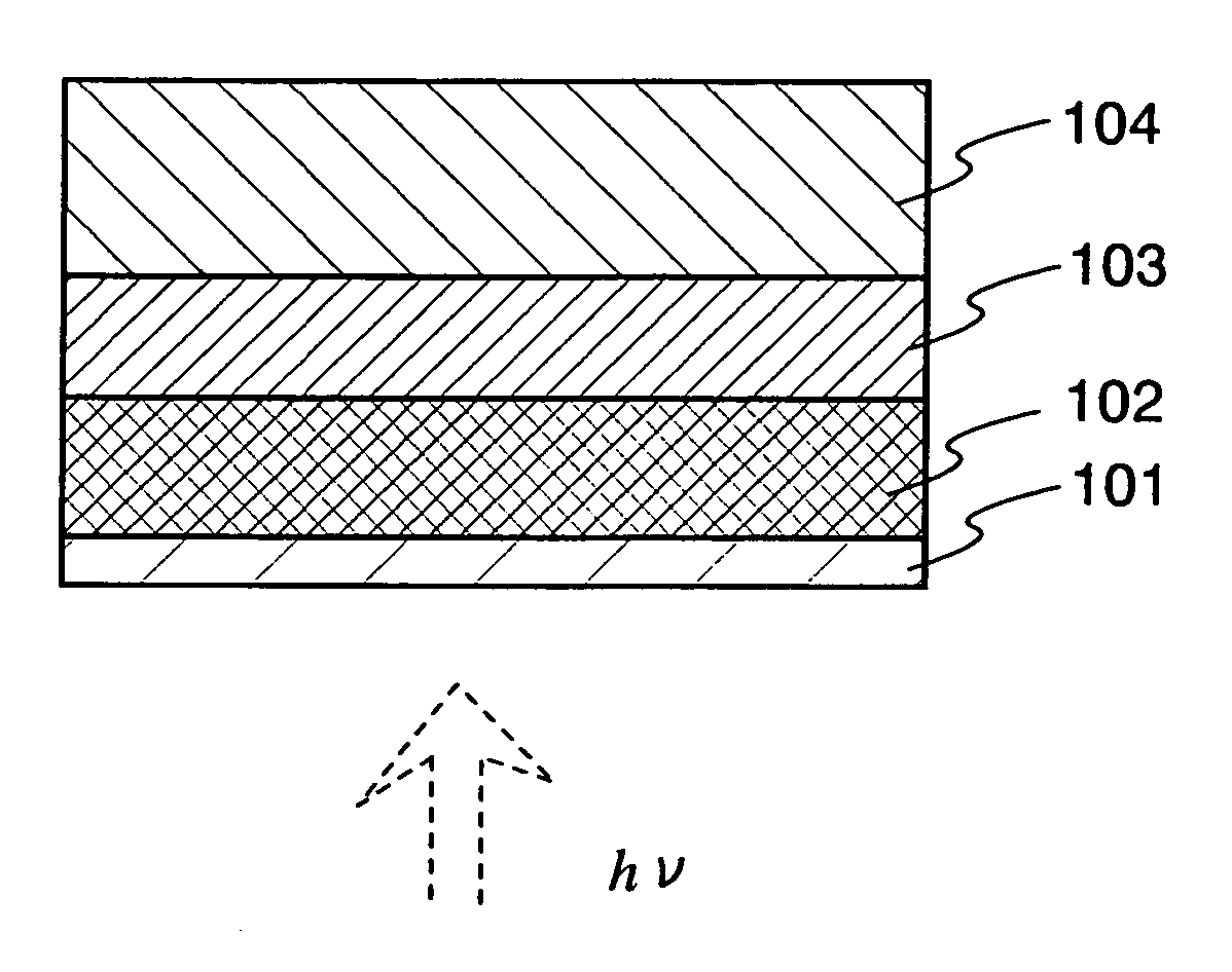
[0044]FIG. 1 shows an element structure of a photoelectric conversion element of the invention. Here, a charge generating layer is formed of a layer containing an organic compound and an inorganic compound each of which has a hole transporting property and a charge acceptor layer is formed of an organic compound having an electron transporting property.

[0045] The photoelectric conversion element has a stacked-layer structure in which a first electrode 101, a charge generating layer 102, a charge acceptor layer 103, and a second electrode 104 are sequentially stacked.

[0046] The first electrode 101 is formed of a material which is conductive and has high light transmissivity against a wavelength region of an incident excited light. The first electrode 101 is formed by a vacuum vapor deposition method, a sputtering method and the like, and a thickness thereof is not limited. It is preferable to use a metal and a metal oxide, in particular Al, indium tin oxide (ITO), SnO2, and In2O3 c...

embodiment mode 2

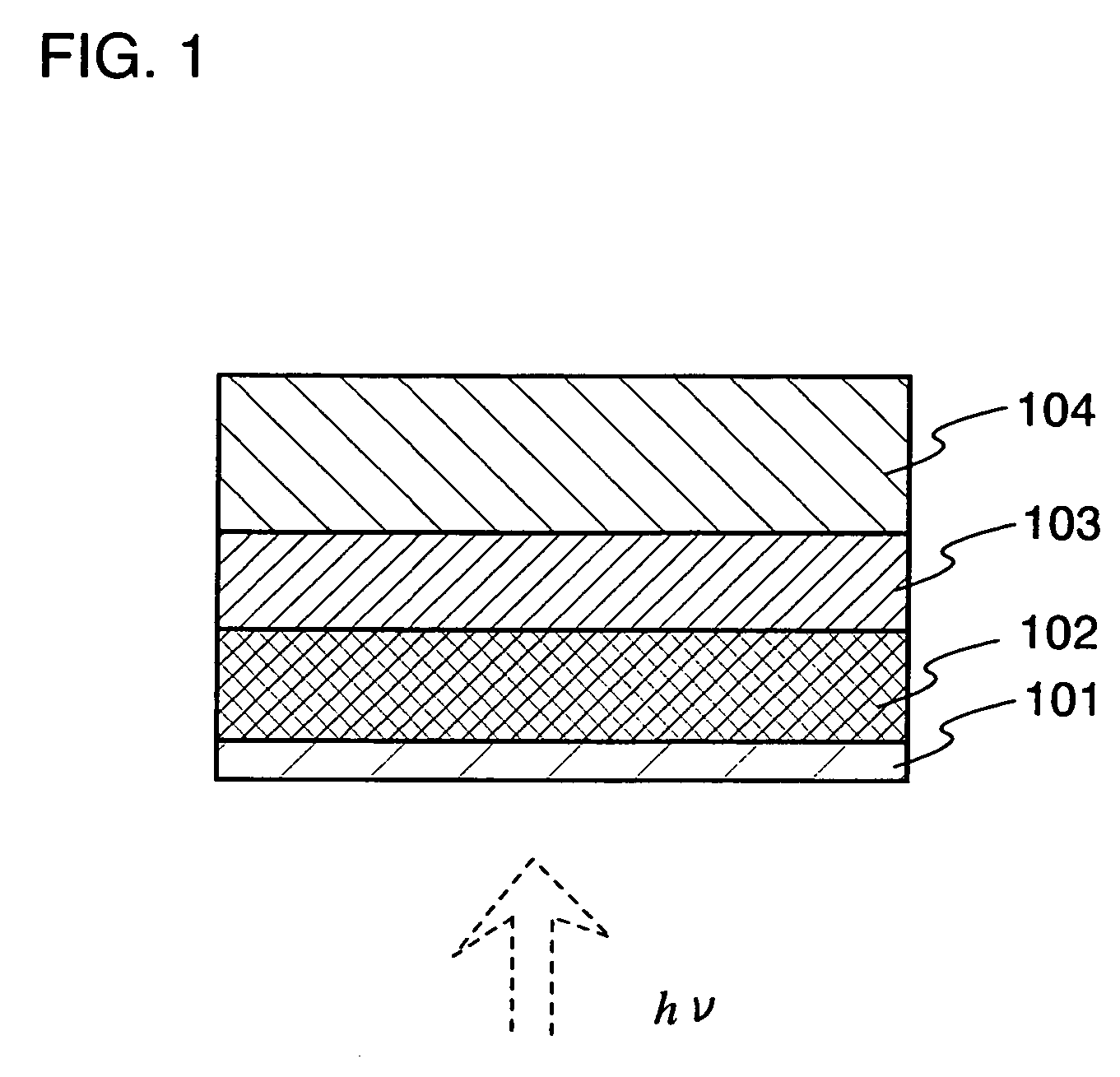
[0058]FIG. 2 shows an element structure of a photoelectric conversion element. Here, a charge generating layer is formed of a layer containing an organic compound and an inorganic compound each of which has an electron transporting property and a charge acceptor layer is formed of an organic compound having a hole transporting property.

[0059] A charge acceptor layer 202 is formed over the first electrode 101 and a charge generating layer 203 is formed over the charge acceptor layer 202.

[0060] The charge generating layer 203 is formed of an organic compound and an inorganic compound each of which has an electron transporting property. The organic compound having an electron transporting property may be formed of the substance having an electron transporting property specifically described in Embodiment Mode 1. The inorganic compound is preferably formed of a metal oxide or a metal nitride each of which shows an electron donating property to the first organic compound, and more pref...

embodiment mode 3

[0062]FIG. 3 shows an element structure of a photoelectric conversion element and a solar battery of the invention. Here, a first charge generating layer is formed of a layer containing an organic compound having a hole transporting property and a first inorganic compound. A second charge generating layer is formed of a layer containing an organic compound having an electron transporting property and a second inorganic compound.

[0063] A first charge generating layer 302 is formed over the first electrode 101 and a second charge generating layer 303 is formed over the first charge generating layer 302.

[0064] The first charge generating layer 302 may be formed of the substance of the charge generating layer 102 specifically described in Embodiment Mode 1. The second charge generating layer 303 may be formed of the substance of the charge generating layer 203 specifically described in Embodiment Mode 2.


PUM


Abstract

The invention provides a photoelectric conversion element and a solar battery having the photoelectric conversion element each of which has a structure with a high carrier generating rate. Further, the invention provides a photoelectric conversion element and a solar battery having the photoelectric conversion element of which high energy converting efficiency. According to the invention, the photoelectric conversion element and the solar battery having the photoelectric conversion element are characterized in that a pair of electrodes sandwich a mixed layer including a charge generating layer and a charge acceptor layer. The charge generating layer is formed of a first organic compound and an inorganic compound. The charge acceptor layer is formed of a second organic compound.

Description

BACKGROUND OF THE INVENTION [0001] 1. Field of the Invention [0002] The present invention relates to a photoelectric conversion element, a solar battery, and a photo sensor. [0003] 2. Description of the Related Art [0004] As a photoelectric conversion element and a solar battery having the photoelectric conversion element which convert an optical energy into an electrical energy, a single crystalline silicon solar battery as a first generation, a polycrystalline silicon solar battery formed of a number of crystals as a second generation, and a compound semiconductor solar battery using gallium arsenic and the like as a third generation have been suggested, although they have many problems in cost and the like. In view of this, a solar battery formed of an organic semiconductor is suggested. [0005] An organic semiconductor solar battery is typically a dye thin film solar battery and a dye-sensitization solar battery. A dye thin film solar battery has a p-n heterojunction structure us...

Claims


Application Information

Patent Timeline
IPC IPC(8): H01L31/00
CPCH01L51/422H01L51/4246H01L51/4253Y02E10/549H10K30/15H10K30/211H10K30/30
Inventor IWAKI, YUJI
Owner SEMICON ENERGY LAB CO LTD
Why Eureka
Try Eureka