Photoelectric conversion device and method of manufacturing the same

a technology photoelectric conversion device, which is applied in the direction of sustainable manufacturing/processing, climate sustainability, semiconductor devices, etc., can solve the problems of low photoelectric conversion efficiency of photoelectric conversion device using crystal semiconductor particles, difficult to apply pastes to photoelectric conversion devices, etc., and achieves high photoelectric conversion efficiency and power generation efficiency of photoelectric apparatus.

Inactive Publication Date: 2006-06-08
KYOCERA CORP
View PDF4 Cites 11 Cited by
  • Summary
  • Abstract
  • Description
  • Claims
  • Application Information

AI Technical Summary

Benefits of technology

[0024] A photoelectric apparatus according to the present invention uses the photoelectric conversion device according to the present invention as power generation means and is configured so as to supply power generated by the power generation means to a load. Since the photoelectric apparatus uses the photoelectric conversion device having high photoelectric conversion efficiency is used, the power generation efficiency of the photoelectric apparatus can be improved.

Problems solved by technology

It has been difficult to apply the pastes to a photoelectric conversion device of a ball solar type in which crystal semiconductor particles are aligned with one another and are welded to an aluminum substrate.
In the photoelectric conversion device using the crystal semiconductor particles, therefore, it has been impossible to improve the BSF effect.
Therefore, the photoelectric conversion device using the crystal semiconductor particles has been low in photoelectric conversion efficiency.

Method used


Image

  • Photoelectric conversion device and method of manufacturing the same
  • Photoelectric conversion device and method of manufacturing the same
  • Photoelectric conversion device and method of manufacturing the same

Examples


example 1

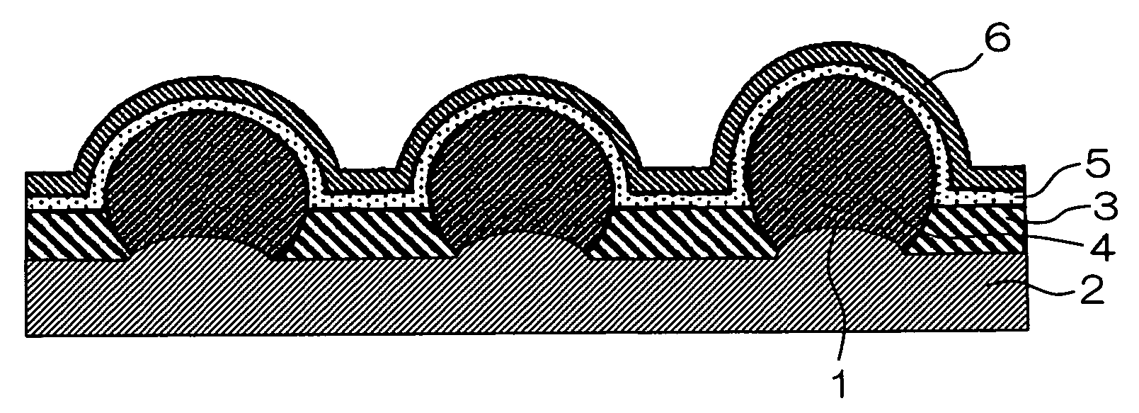
[0079] A conductive substrate 2 of aluminum quality whose boron content is changed into various values was degreased using a sodium hydroxide (NaOH) solution and was then neutralized using a nitric acid (HNO3) solution, to clean its surface. A plurality of p-type crystal semiconductor particles 4 composed of p-type silicon particles having a diameter of about 0.5 mm from which a surface oxide layer was removed using a hydrofluoric acid (HF) solution were arranged on the conductive substrate 2, and were heated at 600 to 630° C. for one to ten minutes, to diffuse and join a lower part of each of the p-type crystal semiconductor particles 4 into and to the conductive substrate 2.

[0080] Polyimide was then used as an insulator 3, was applied so as to have a thickness of about 100 μm between the p-type crystal semiconductor particles 4, was dried at 200° C. for thirty minutes, and was then calcined at 350° C. for one hour, to form the layered insulator 3.

[0081] An n-type semiconductor l...

example 2

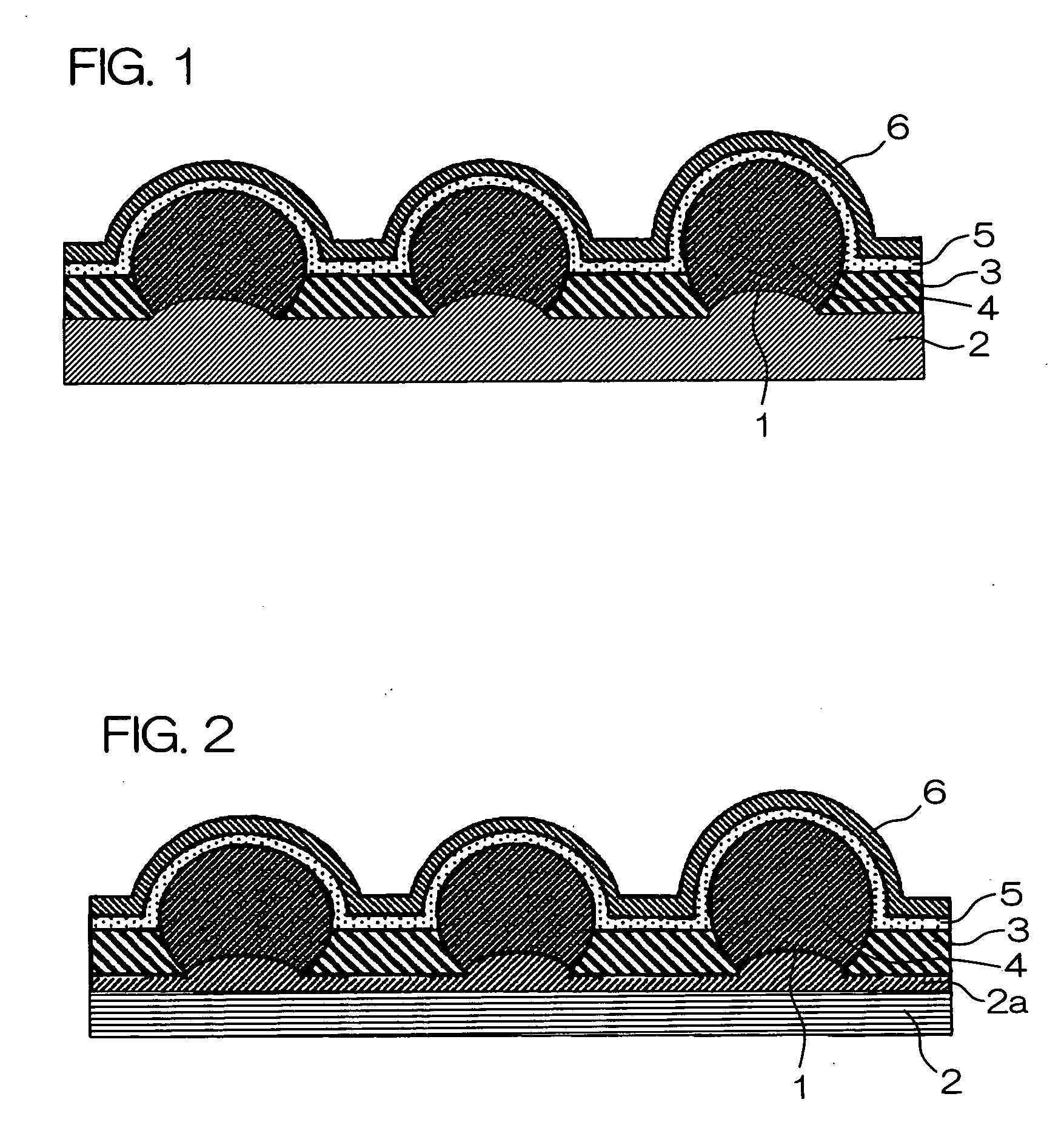
[0088] A boric acid solution whose boron concentration is changed into various values was applied to a conductive substrate 2 of aluminum quality whose surface was cleaned by being degreased using a sodium hydroxide solution and then neutralized using a nitric acid solution, followed by drying, to produce conductive substrates 2 respectively having boron compound layers 2c that differ in amount of boron per unit area. A plurality of p-type silicon particles having a diameter of about 0.5 mm from which a surface oxide layer was removed using a hydrofluoric acid solution were arranged on the boron compound layer 2c, and were heated at 600 to 630° C. for one to ten minutes, to diffuse and join a lower part of each of the p-type silicon particles into and to the conductive substrate 2.

[0089] Polyimide was then used as an insulator 3, was applied so as to have a thickness of about 100 μm between the p-type silicon particles, was dried at 200° C. for thirty minutes, and was then calcined...

example 3

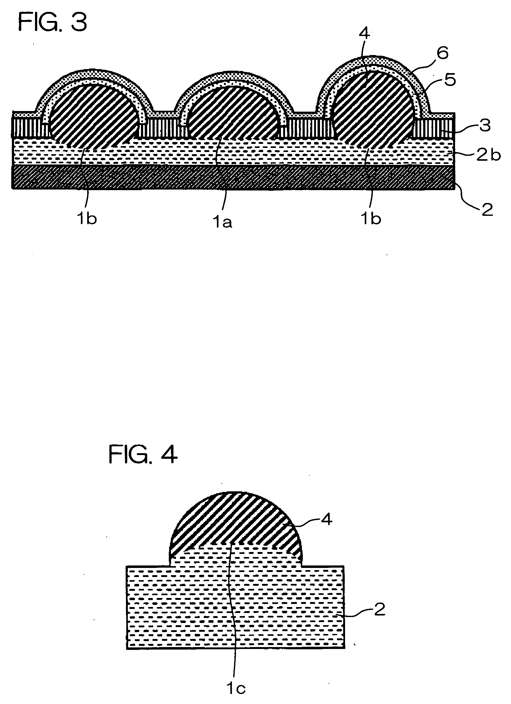
[0093] A surface of each of p-type crystal semiconductor particles 4 having an average particle diameter of 400 μm to which a small amount of boron (B) was added as a p-type dopant was washed, followed by thermal diffusion at 850° C. for thirty minutes in a POCl3 atmosphere, to form an n-type silicon layer as an n-type semiconductor layer 5 on the surface of the p-type crystal semiconductor particle 4. At this time, a portion into which boron is not diffused was covered with silicon oxide, to form an n-type silicon layer in only a necessary portion.

[0094] One layer of p-type crystal semiconductor particles 4 each having an n-type silicon layer formed therein was then densely disposed on the conductive substrate 2 made of aluminum, to change diffusion and junction conditions such as junction temperature, junction time, temperature rise speed, and temperature fall speed in various ways, thereby producing samples in which the conductive substrate 2 and the p-type crystal semiconductor...


PUM

PropertyMeasurementUnit
thicknessaaaaaaaaaa
temperatureaaaaaaaaaa
thicknessaaaaaaaaaa

Abstract

Disclosed is a photoelectric conversion device in which a plurality of p-type crystal semiconductor particles 4 are joined to one main surface of a conductive substrate 2. A boron concentration in a junction of a lower part of each of the p-type crystal semiconductor particles 4 with the conductive substrate 2 is higher than a boron concentration in a portion, other than the junction, of the p-type crystal semiconductor particle 4. The junction is a p+ layer having a high impurity concentration. The p+ layer allows p-type carriers to be collected, thereby making it possible to improve a BFS effect.

Description

BACKGROUND OF THE INVENTION [0001] 1. Field of the Invention [0002] The present invention relates to a photoelectric conversion device used for solar photoelectric generation or the like, and more particularly, to a photoelectric conversion device using crystal semiconductor particles and a method of manufacturing the same. [0003] 2. Description of Related Art [0004] Conventional photoelectric conversion elements using general crystal semiconductors are so configured that an n-type semiconductor region is formed on one main surface of a p-type silicon substrate to form a pn junction, and electrodes are respectively formed on the transparent electrode and the other main surface of the p-type silicon substrate. [0005] In recent years, an output of a solar cell has been strongly required to be improved. As one measure to improve the output of the solar cell, it has been desired to improve a BSF (Back Surface Field) effect. For this purpose, a p+ layer has been formed in the interface o...

Claims


Application Information

Patent Timeline
Patent Type & Authority Applications(United States)
IPC IPC(8): H01L31/06
CPCH01L31/02167H01L31/0288H01L31/035281H01L31/03529H01L31/1804Y02E10/547Y02P70/50
Inventor UCHIMOTO, KOUICHIFUKUDA, JUNHAKUMA, HIDEKISUGAWARA, SHINARIMUNE, HISAO
Owner KYOCERA CORP
Why Eureka
Try Eureka