Mask making method, mask making device, and mask drawing device
a mask and making device technology, applied in the field of mask making methods, mask making devices, and mask drawing devices, can solve the problems of difficult to enhance the accuracy of such movement, difficult to provide or prepare a number of such systems, and high mask writing price, so as to improve stitching accuracy, high speed, and high accuracy.
- Summary
- Abstract
- Description
- Claims
- Application Information
AI Technical Summary
Benefits of technology
Problems solved by technology
Method used
Image
Examples
first embodiment
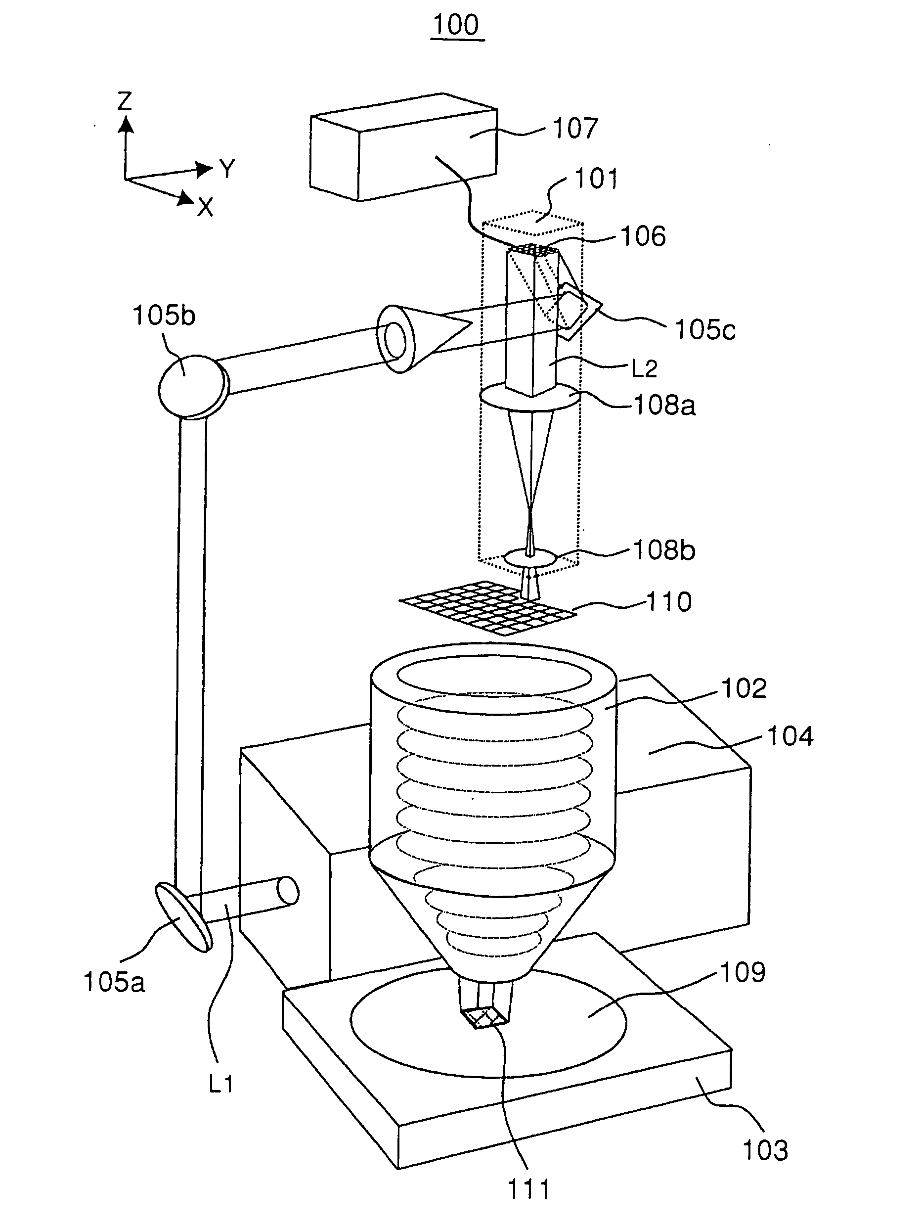
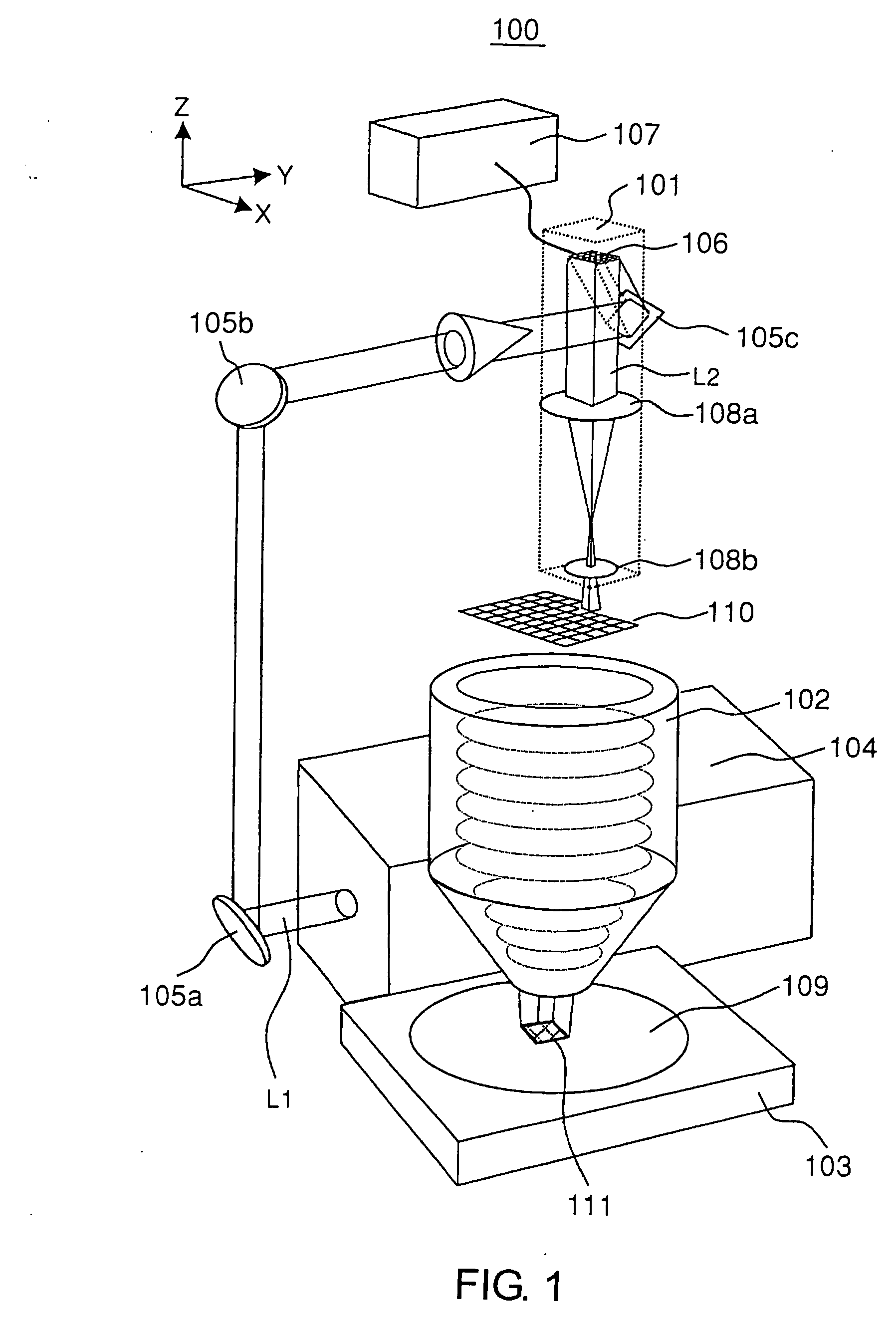
[0030]FIG. 1 is a structural diagram of a mask writing system 100 according to this invention. The mask writing system 100 comprises an enlarged-pattern generating portion 101 having a two-dimensional array micromirror 106 that can form an optional pattern, a reduction-projection optical system 102, a stage 103 having a mask substrate 109 placed thereon, and an ultraviolet laser oscillator 104 for generating laser light L1 in the ultraviolet wavelength region to which a resist applied to the mask substrate 109 is sensitive.
[0031] The laser light L1 extracted from the ultraviolet laser oscillator 104 is reflected by mirrors 105a and 105b and is projected onto a mirror 105c in the enlarged-pattern generating portion 101 so as to be irradiated onto the two-dimensional array micromirror 106.
[0032] In the two-dimensional array micromirror 106, micromirrors are individually controlled by data given from a mask pattern data output device 107 so that the micromirrors are controlled to form...
second embodiment
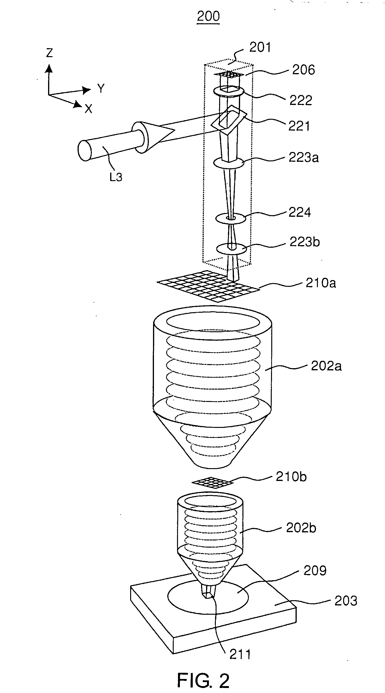
[0040]FIG. 2 is a structural diagram of a mask writing system 200 according to this invention. As compared with the mask writing system 100 shown in FIG. 1, this embodiment differs in two points which will be described hereinbelow. The other basic structure is the same. Although use is made of an ultraviolet laser oscillator for generating laser light in the ultraviolet region and a pattern data output device, they are omitted in FIG. 2. The different points are a control system for ultraviolet laser light in an enlarged-pattern generating portion 202 and a structure of a reduction-projection optical system.
[0041] Laser light L3 is incident upon a beam splitter 221 in the enlarged-pattern generating portion 202 and is reflected upward to pass through a wavelength plate 222 so as to be incident upon a two-dimensional array micromirror 206. Laser light reflected by micromirrors corresponding to a pattern forming part of an intended mask lithography pattern in the two-dimensional array...
third embodiment
[0045]FIG. 3 is a structural diagram of a mask writing system 300 according to this invention. In the mask writing system 300, a two-dimensional array self-light-emitting device 306 is used as light control elements arranged in a two-dimensional array, which forms this invention. In the two-dimensional array self-light-emitting device 306, only those elements corresponding to a pattern of part of an intended mask lithography pattern are caused to emit light. Then, a light-emission pattern thereof is reduced through a first reduction-projection optical system 302a and a second enlarged pattern 310b is reduced through a second reduction-projection optical system 302b so that a lithography pattern 311 is formed on a mask substrate 309 on a stage 303. The two-dimensional array self-light-emitting device 306 can be scanned in X- and Y-directions in the figure, thereby constituting a first enlarged pattern 310a formed with the entire lithography pattern.
[0046] As the two-dimensional array...
PUM
 Abstract
Description
Claims
Application Information


