Low refractive index polymers as underlayers for silicon-containing photoresists

a technology of low refractive index and polymer, which is applied in the direction of auxillary/base layers of photosensitive materials, instruments, photosensitive materials, etc., can solve the problems of low etch resistance of polymer layer under the underlayer, and inapplicability to 193 nm lithographic applications, etc., to achieve high etch resistance and improve optical properties

Inactive Publication Date: 2006-06-22
GLOBALFOUNDRIES INC
View PDF36 Cites 20 Cited by
  • Summary
  • Abstract
  • Description
  • Claims
  • Application Information

AI Technical Summary

Benefits of technology

[0012] It is an object of the invention to provide a new underlayer composition that exhibits high etch resistance and improved optical properties.

Problems solved by technology

Thinning of a conventional single layer resist to improve resolution generally results in compromise of the etch resistance of the resist which is needed to transfer the desired image to the underlying material layer.
These materials very strongly absorb 193 nm radiation, thus are not suitable for 193 nm lithographic applications.
One drawback of lower ratio of aromatic moieties is that the resulting polymer would have lower etch resistance for patterning the material layer under the underlayer.
The other drawback is that it would be very difficult to get the right optical properties in the synthetic process, such as rendering the polymer either too high in absorption when too much aromatic moieties are incorporated, or too low in absorption when not enough aromatic moieties are incorporated.
It is very difficult to tune the n and k values with this rigid composition.

Method used


Image

  • Low refractive index polymers as underlayers for silicon-containing photoresists
  • Low refractive index polymers as underlayers for silicon-containing photoresists
  • Low refractive index polymers as underlayers for silicon-containing photoresists

Examples


example 1

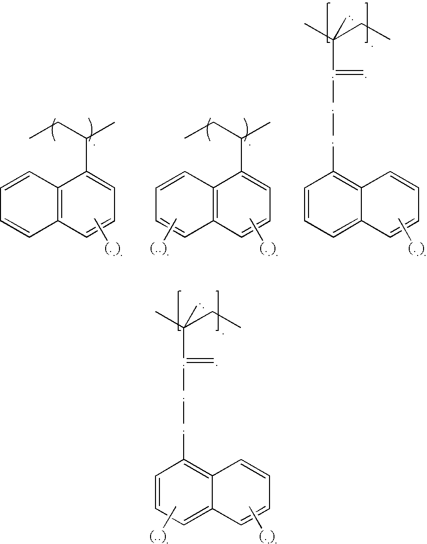
Synthesis of copolymer of 2-vinylnaphthalene and 5-hydroxy-1-naphthalenyl methacrylate (VN / HNM(60 / 40))

[0044] 1.01 g of 2-vinylnaphthalene, 1 g of 5-hydroxy-1-naphthalenyl methacrylate and 90 mg of 2,2′-azobis(2-methylpropionitrile) (AlBN) initiator were dissolved in 8.4 g of tetrahydrofuran (THF) and charged into a 3-neck flask. The system was then purged with N2 for 30 minutes before the temperature was raised to 70° C. The reaction was carried out under N2 overnight at 70° C. The solution was then precipitated in 1000 ml of deionized (DI) water. The polymer was collected and dried in vacuum oven overnight at 65° C. Yield was 96%.

example 2

Synthesis of terpolymer of 2-vinylnaphthalene, 5-hydroxy-1-naphthalenyl methacrylate and hydroxyethyl methacrylate (VN / HNM / HEMA(37.5 / 37.5 / 25))

[0045] 0.68 g of 2-vinylnaphthalene, 1.01 g of 5-hydroxy-1-naphthalenyl methacrylate, 0.38 g of hydroxyethyl methacrylate and 101 mg of AlBN initiator were dissolved in 10.8 g of THF and charged into a 3-neck flask. The system was then purged with N2 for 30 minutes before the temperature was raised to 72° C. The reaction was carried out under N2 overnight at 72° C. The solution was then precipitated in 1000 ml of DI water. The polymer was collected and dried in vacuum oven overnight at 65° C. Yield was >90%.

example 3

Synthesis of homopolymer of 5-hydroxy-1-naphthalenyl methacrylate (HNM)

[0046] 1.0 g of 5-hydroxy-1-naphthalenyl methacrylate and 36 mg of AlBN initiator were dissolved in 6 g of THF and charged into a 3-neck flask. The system was then purged with N2 for 30 minutes before the temperature was raised to 72° C. The reaction was carried out under N2 overnight at 72° C. The solution was then precipitated in 2000 ml of DI water. The polymer was collected and dried in vacuum oven overnight at 65° C.


PUM

PropertyMeasurementUnit
wavelengthaaaaaaaaaa
reflectivityaaaaaaaaaa

Abstract

A new underlayer composition that exhibits high etch resistance and improved optical properties is disclosed. The underlayer composition comprises a vinyl or acrylate polymer, such as a methacrylate polymer, the polymer comprising at least one substituted or unsubstituted naphthalene or naphthol moiety, including mixtures thereof. Examples of the polymer of this invention include:
where each R1 is independently selected from an organic moiety or a halogen; each A is independently a single bond or an organic moiety; R2 is hydrogen or a methyl group; and each X, Y and Z is an integer of 0 to 7, and Y+Z is 7 or less. The organic moiety mentioned above may be a substituted or unsubstituted hydrocarbon selected from the group consisting of a linear or branched alkyl, halogenated linear or branched alkyl, aryl, halogenated aryl, cyclic alkyl, and halogenated cyclic alkyl, and any combination thereof. The compositions are suitable for use as a planarizing underlayer in a multilayer lithographic process, including a trilayer lithographic process.

Description

BACKGROUND OF THE INVENTION [0001] 1. Field of the Invention [0002] This invention relates to an underlayer composition for silicon-containing photoresists, especially silicon-containing multilayer resists. More particularly, this invention relates to an underlayer composition that comprises a vinyl or acrylate polymer comprising a naphthalene moiety or naphthol moiety. [0003] 2. Description of the Related Art [0004] In the microelectronics industry, there is a continued desire to reduce the size of structural features and / or to provide greater amount of circuitry for a given chip size. Advanced lithographic techniques are required to fabricate high performance and high density circuitry. Lithography impacts the manufacture of microscopic structures not only in terms of directly imaging patterns on the desired substrate, but also in terms of making masks typically used in such imaging. [0005] The resolution capability of lithographic processes is generally a function of the waveleng...

Claims


Application Information

Patent Timeline
Patent Type & Authority Applications(United States)
IPC IPC(8): G03C1/76
CPCG03F7/091G03F7/094Y10S438/952
Inventor HUANG, WU-SONGBURNS, SEAN D.KHOJASTEH, MAHMOUD
Owner GLOBALFOUNDRIES INC
Why Eureka
Try Eureka