Supercharge Your Innovation With Domain-Expert AI Agents!

Interface engineering to improve adhesion between low k stacks

Active Publication Date: 2006-07-20
APPLIED MATERIALS INC
View PDF19 Cites 36 Cited by
  • Summary
  • Abstract
  • Description
  • Claims
  • Application Information

AI Technical Summary

Benefits of technology

[0009] The present invention generally provides a method for depositing an organosilicate dielectric layer comprising sequentially depositing a silicon oxide layer having low carbon content and a carbon doped silicon oxide layer having a low dielectric constant within the same processing chamber without plasma arcing. In one embodiment, the method for depositing an organosilicate dielectric layer includes flowing an interface gas mixture comprising one or more organosilicon compounds and one or more oxidizing gases through a gas distribution plate, such as a showerhead, to a substrate surface at first deposition conditions, wherein a high frequency RF (HFRF) bias is applied to a powered electrode, such as the showerhead, to deposit a silicon oxide interface layer having less than about 3 atomic percent carbon, then increasing the flow rate of the one or more organosilicon compounds while depositing a transition layer on the interface layer, and then flowing a final gas mixture to deposit a carbon doped silicon oxide layer having at least 10 atomic percent carbon. Changing process conditions as described herein substantially reduces variation of DC bias of the powered electrode to a variation less than 60 volts during processing.

Problems solved by technology

However, one problem that has been encountered with plasma processing in integrated circuit fabrication is device damage that occurs as a result of exposure of a device to non-uniform plasma conditions, such as electric field gradients caused by changing process conditions.
While the susceptibility or degree of device damage typically depends at least partially on the stage of device fabrication and the type of device, many types and stages of devices can experience plasma-induced damage (PID).
For example, a substrate that has a barrier layer or dielectric layer deposited thereon is more susceptible to PID due to the accumulation of surface charge, and a buildup of potential gradients during processing.
Furthermore, as the size of devices become smaller and the dielectric layers become increasingly thinner, devices are becoming increasingly susceptible to PID.
Inadequate adhesion may result in delamination of the low-k dielectric layer from the underlying substrate and potential failure of the device.
Furthermore, the deposition of a thin silicon oxide layer prior to deposition of a carbon doped silicon oxide layer substantially increases processing time unless the layers are deposited sequentially in the same chamber.
Sequential deposition has resulted in plasma arcing when the deposition conditions are changed.
The plasma arcing damages the substrate surface and effectively negates any advantage in depositing the thin silicon oxide film and the carbon doped silicon oxide layer in the same chamber.

Method used


Image

  • Interface engineering to improve adhesion between low k stacks
  • Interface engineering to improve adhesion between low k stacks
  • Interface engineering to improve adhesion between low k stacks

Examples


example

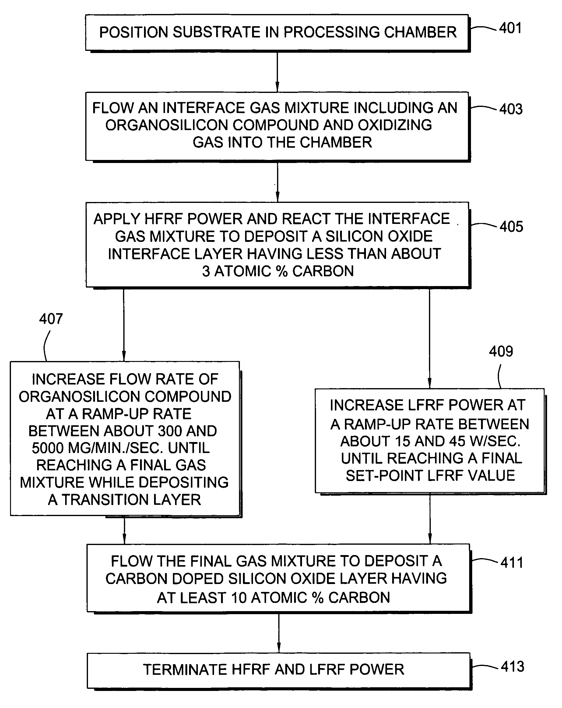
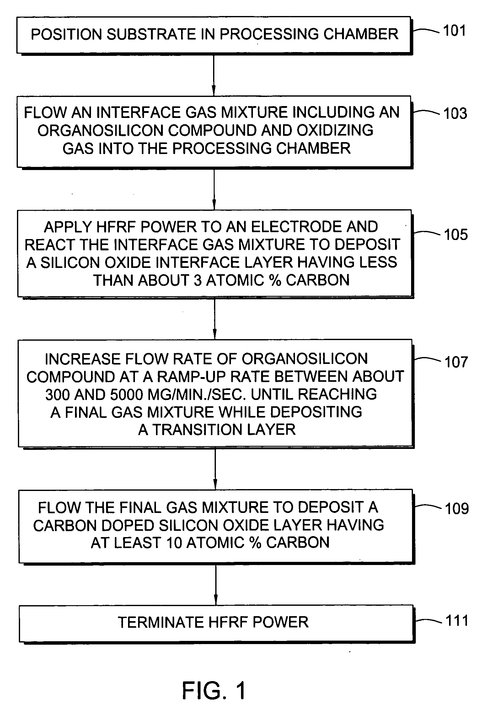
[0048] Organosilicate dielectric layers were deposited on a substrate in accordance with the embodiment described above with respect to FIG. 5. The films were deposited using a PECVD chamber (i.e., CVD chamber) on a PRODUCER system, available from Applied Materials, Inc. of Santa Clara, Calif. During deposition the chamber pressure was maintained at a pressure of about 4.5 Torr and the substrate was maintained at a temperature of about 350° C.

[0049] The substrate was positioned on a substrate support disposed within a process chamber. The process gas mixture having an initial gas composition of 1000 sccm helium and 700 sccm oxygen for the interface layer was introduced into the chamber and flow rates stabilized before initiation of the HFRF power. Subsequently, HFRF power of about 500 W was applied to the showerhead to form a plasma of the interface process gas mixture composition including a OMCTS flow rate of about 700 mg / min., and deposit a silicon oxide layer having a carbon co...


PUM

PropertyMeasurementUnit
Poweraaaaaaaaaa
Poweraaaaaaaaaa
Poweraaaaaaaaaa

Abstract

A method of depositing a organosilicate dielectric layer exhibiting high adhesion strength to an underlying substrate disposed within a single processing chamber without plasma arcing. The method includes positioning a substrate within a processing chamber having a powered electrode, flowing an interface gas mixture into the processing chamber, the interface gas mixture comprising one or more organosilicon compounds and one or more oxidizing gases, depositing a silicon oxide layer on the substrate by varying process conditions, wherein DC bias of the powered electrode varies less than 60 volts.

Description

CROSS-REFERENCE TO RELATED APPLICATIONS [0001] This application claims benefit of U.S. Provisional Patent Application Ser. No. 60 / 644,899, filed Jan. 19, 2005, which is herein incorporated by reference. This application is also related to U.S. patent application Ser. No. 10 / 645,675, filed Aug. 20, 2003 which is herein incorporated by reference.BACKGROUND OF THE INVENTION [0002] 1. Field of the Invention [0003] Embodiments of the present invention generally relate to the fabrication of integrated circuits. More particularly, embodiments of the present invention relate to a method for depositing organosilicate layers on a substrate. [0004] 2. Description of the Related Art [0005] In the manufacture of integrated circuits, plasma processes are increasingly being used to replace thermal processes. Plasma processing provides several advantages over thermal processing. For example, plasma enhanced chemical vapor deposition (PECVD) allows deposition processes to be performed at substantial...

Claims


Application Information

Patent Timeline
IPC IPC(8): H01L21/31
CPCC23C16/029C23C16/401C23C16/45523C23C16/5096H01L21/02126H01L21/02216H01L21/02274H01L21/31633H01L21/02211H01L21/02164H01L21/31
Inventor PADHI, DEENESHBALASUBRAMANIAN, GANESHLAKSHMANAN, ANNAMALAICUI, ZHENJIANGROCHA-ALVAREZ, JUAN CARLOSKIM, BOK HOENM'SAAD, HICHEMREITER, STEVENSCHMITT, FRANCIMAR
Owner APPLIED MATERIALS INC
Features
  • R&D
  • Intellectual Property
  • Life Sciences
  • Materials
  • Tech Scout
  • Unparalleled Data Quality
  • Higher Quality Content
  • 60% Fewer Hallucinations
Learn More