Silicon member and method of manufacturing the same

Inactive Publication Date: 2006-08-03
COVALENT MATERIALS CORP +1
View PDF5 Cites 7 Cited by
  • Summary
  • Abstract
  • Description
  • Claims
  • Application Information

AI Technical Summary

Benefits of technology

[0029] In the above-mentioned method for manufacturing a silicon member, from the viewpoint of easily controlling the intrinsic resistivity of the a

Problems solved by technology

Such a change in the resistivity of the silicon member as described above is frequently caused in a process to cause loss and variation in an electric field in the system to make wafer processing uneven to further cause a reduction in yield, which is not preferable.
Moreover, in recent years, as devices have become more complicated and more sophisticated, circuit patterns formed on wafers have become finer.
Also in this sputtering, in the case of using an N-type silicon member, it is thought that there is a large possibility that phosphorus or arsenic of the do

Method used


Image

  • Silicon member and method of manufacturing the same
  • Silicon member and method of manufacturing the same

Examples


embodiment

[0062] Hereinafter, the present invention will be described more specifically based on embodiment, but the present invention is not limited by the following embodiment.

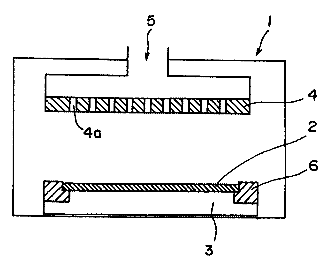
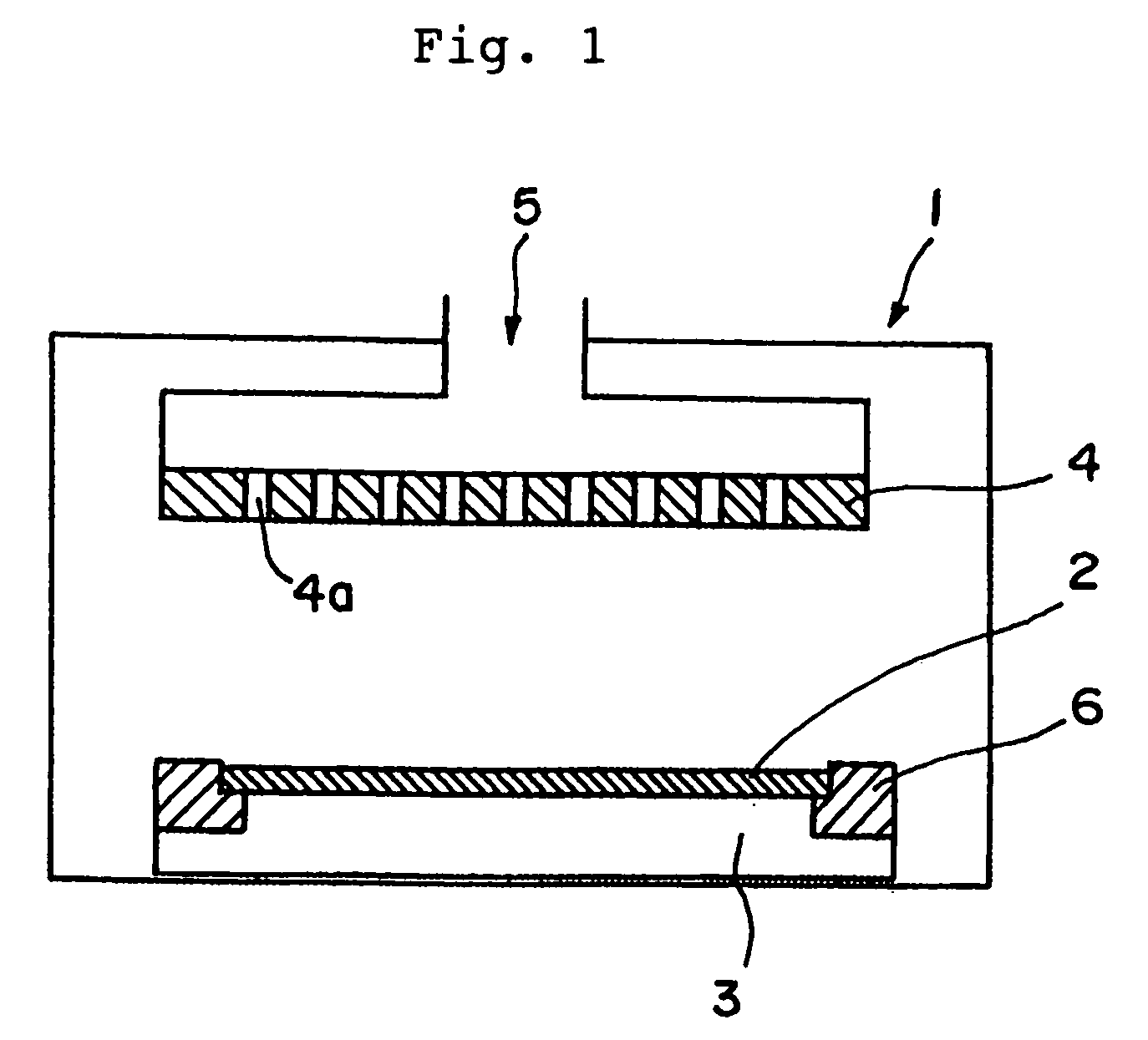
[0063] A P-type silicon single crystal doped with boron at a concentration of 1.72×10¹⁵ atoms / cm3 (having an intrinsic resistivity of 7.7 Ω·cm and a resistivity of 12.1 Ω·cm) was worked into a focus ring (having an outside diameter of 360 mm, an inside diameter of 302 mm, and a thickness of 5 mm), as shown in FIG. 1.

[0064] Thereafter, this was subjected to annealing processing under argon atmosphere at 470° C. for 15 hours, thereby being changed in its conduction type from a P type into an N type. In this manner, a focus ring made of an N-type silicon single crystal was manufactured.

[0065] The study of characteristics of the produced focus ring revealed that the focus ring had a resistivity of 2.7 Ω·cm and an oxygen concentration of 1.5×10¹⁸ atoms / cm3.


PUM


Abstract

There is provided a silicon member that can prevent the resistivity of a member itself from varying in a semiconductor manufacturing process, in particular, in a plasma processing process, thereby making wafer processing uniform and being not an impurity contamination source to a wafer to be processed, and a method for manufacturing the same. The silicon member having a resistivity of 0.1 Ω·cm or more and 100 Ω·cm or less is manufactured with steps which are manufacturing a P-type silicon single crystal doped with 13 group atoms of a periodic table having an intrinsic resistivity of 1 Ω·cm or more and 100 Ω·cm or less, and changing said P-type silicon single crystal into an N-type silicon single crystal by oxygen donors formed by annealing at a temperature of 300° C. or more and 500° C. or less.

Description

BACKGROUND OF THE INVENTION [0001] 1. Field of the Invention [0002] The present invention relates to a silicon member that can be suitably used for plasma etching processing and heat treatment in a semiconductor manufacture. [0003] 2. Description of the Related Art [0004] In a semiconductor manufacturing process, for example, a plasma etching apparatus shown in FIG. 1 is used in the process of forming a circuit pattern on a silicon wafer and an oxide film or a nitride film formed on the wafer is subjected to etching processing by producing plasma in a high-frequency electric field. [0005] In a plasma etching apparatus 1 shown in FIG. 1, a wafer 2 is placed on a lower electrode 3 and a reactive gas 5 is supplied from the gas jet ports 4a of a shower plate (upper electrode) 4 and a high-frequency voltage is generated across the electrodes to produce a plasma to etch the surface of the wafer 2. [0006] Here, to etch the wafer 2 uniformly, an electric field needs to be uniformly extended...

Claims


Application Information

Patent Timeline
IPC IPC(8): H01L29/36
CPCH01L21/3225H01L21/30
Inventor MORIYA, MASATAKAKASHIMA, KAZUHIKOMIYANO, SHINICHI
Owner COVALENT MATERIALS CORP
Why Eureka
Try Eureka