However, in the above method, although basic processes of instillation to follow is shown, a specific description relative to a fabrication technology is insufficient and in reality, technical problems remain in practical application of the process.
The instilling process, in comparison to the liquid crystal injection process performed in the past, enables to simply fabricate a liquid crystal panel at low cost but at the same time has technical difficulties as shown below resulting in
delay in adopting the instilling method in a fabrication method of a liquid
crystal display.
If uncured components of the sealing materials 1106 and 1202 make contact with liquid crystal for a long period of time or are exposed in high temperature while contacting with liquid crystal, the liquid crystal is contaminated.
Thus, in the conventional method, a long period of time is required to spread liquid crystal to corner portions of the sealing material 1106 and a
waiting period for curing the sealing material is long.
Accordingly, due to a difference in pressures between the inside and outside of both substrates, possibilities of occurring peeling of corner portions of the sealing material during the
waiting period and generating liquid crystal leakage are high.
However, since vacuum chucks do not function when a degree of vacuum increases to a certain point when the substrates are held by vacuum chucks, the degree of vacuum at the time of attaching substrates can not be sufficiently increased.
Therefore, sufficient pressure for attaching both substrates can not be coated and evenly attaching both substrates is difficult.
Further, in a mechanical holding, since stress is applied only to the holding side portion of a substrate, deformations such as a curvature, deflection and the like occur in a substrate, and both substrates can not be held in parallel when attaching substrates after liquid crystal instillation.
If the attachment is performed when both substrates are deformed, a displacement becomes large and problems of reduction in opening ratio of each
electrode and light leakage from a shaded portion occur.
Accordingly, the above method has a problem of generating display irregularities in which when a formed liquid crystal panel is displayed, the brightness in the two surfaces sandwiching the said boundary varies.
Thus, possibilities of causing a
substrate deformation or contacting the substrates with each other and causing electrostatic destruction exist.
Furthermore, a method in which substrates are held by electrostatic chucks of which the substrate holding strength is not affected by the degree of vacuum also has a problem in which a
glow discharge occurs in the course of decompressing the
atmospheric pressure for attaching substrates and may generate damage to a circuit or a TFT element on a substrate.
Also, a phenomenon may occur in which an operation of the electrostatic chucks becomes unstable due to the air remained between the electrostatic chucks and the substrates, and the substrates break off from the electrostatic chucks in the course of the substrate attachment process.
However, since the amount of liquid crystal to be dropped per one
substrate surface is minute, when dropping positions are scattered into multiple points, an extremely small amount of liquid crystal must be accurately dropped.
However, if the amount of dropped liquid crystal increases, as shown in FIG. 107b, the sealing material 1106 can not be pressed to an intended gap due to excessive liquid crystal resulting in a problem in which display irregularities occur in the
peripheral portion of a panel (periphery of picture-frame portion).
When the amount of dropped liquid crystal is further increased, as shown in FIG. 107c, a phenomenon in which a center portion of a panel is expanded due to the sealing material 1106 causing a press defect occurs resulting in display irregularities on a whole surface.
Further, in a liquid crystal display fabricated by using the instilling method, a problem is generated in which display irregularities occur at the edge of a seal where a sealing material and liquid crystal contact.
However, usually, if a liquid crystal material is irradiated by UV light, characteristics of liquid crystal are degraded, and specifically, resistivity tends to be reduced and
high voltage retention ratio required in TFT-LCD and the like can not be kept.
Further, since an area where the sealing material 1202 before UV
irradiation and the liquid crystal 1206 make contact is large in an instilling method, the possibility of contaminating a liquid crystal material due to uncured sealing material is high.
However, there is a problem in which if a UV light high in strength is irradiated in order to reduce
irradiation time, damage caused by the light leakage to the liquid crystal material also becomes large.
However, even if these techniques are used, the photo-curing process in the instilling method holds problems described below.
However, this method of using a
mask has a problem in which since a
mask is required for each seal pattern and the number of processes is increased by a
mask alignment process, the goal of the instilling method of liquid crystal such as reducing a fabrication cost of a panel and improving
mass productivity may be rather prevented than accomplished.
Thirdly, there is a problem of displacement.
Fourthly, there is a problem of press defect.
However, since the inside of the panel is thicker than a predetermined thickness, the sealing material is subsequently pushed back.
Although the thickness of the panel gradually approaches the predetermined thickness and the sealing material is again pressed to the thickness of a spacer by extending shelf time, liquid crystal is contaminated from uncured sealing material in the time the liquid crystal is left.
Due to this balance, sufficient shelf time can not be taken and insufficient shelf time becomes a cause of generating press defect.
However, in the instilling method, there is a possibility in which a sealing material contacts with liquid crystal when the sealing material is uncured.
In addition to the problems described above, the conventional instilling method further holds problems identified below.
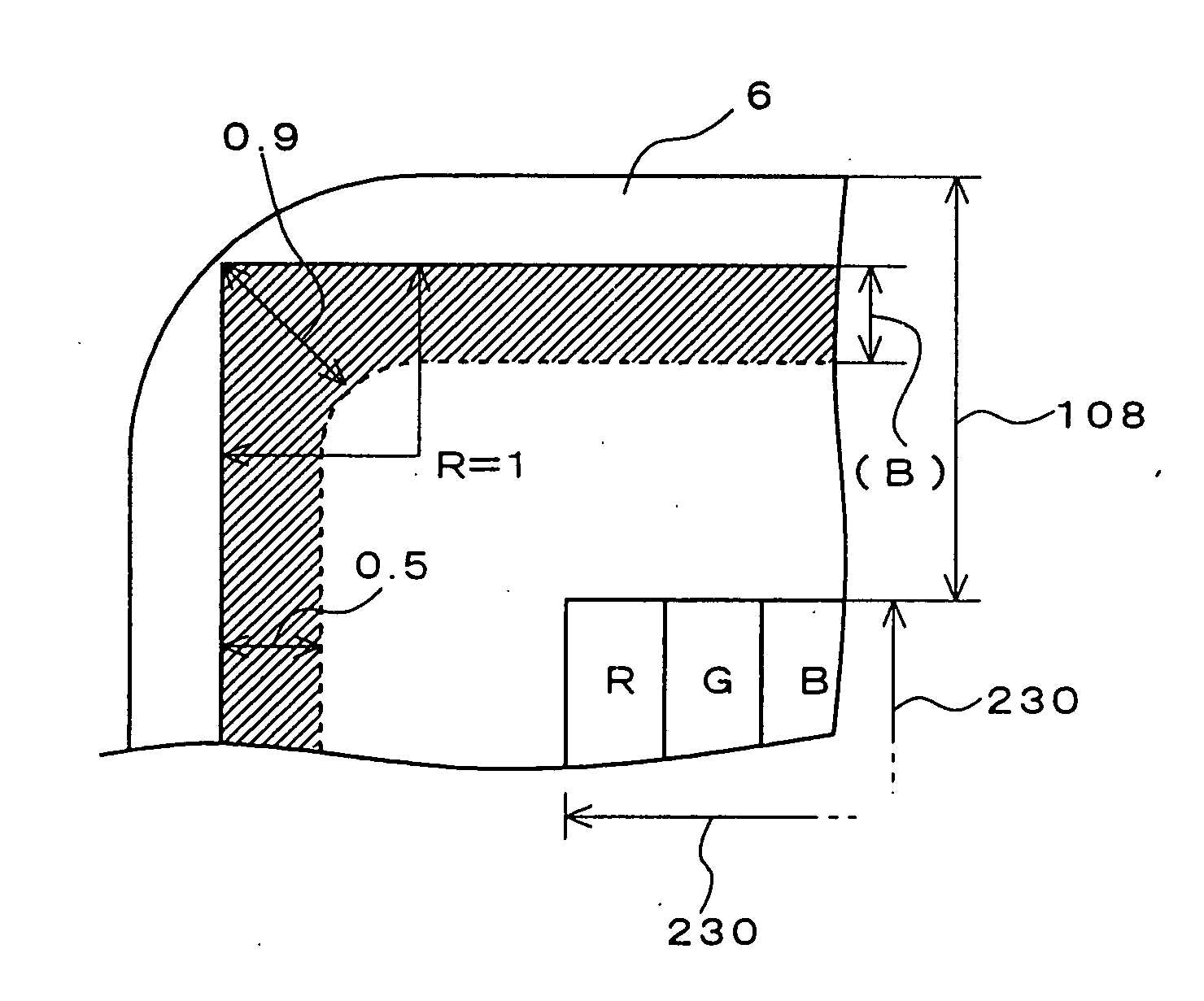
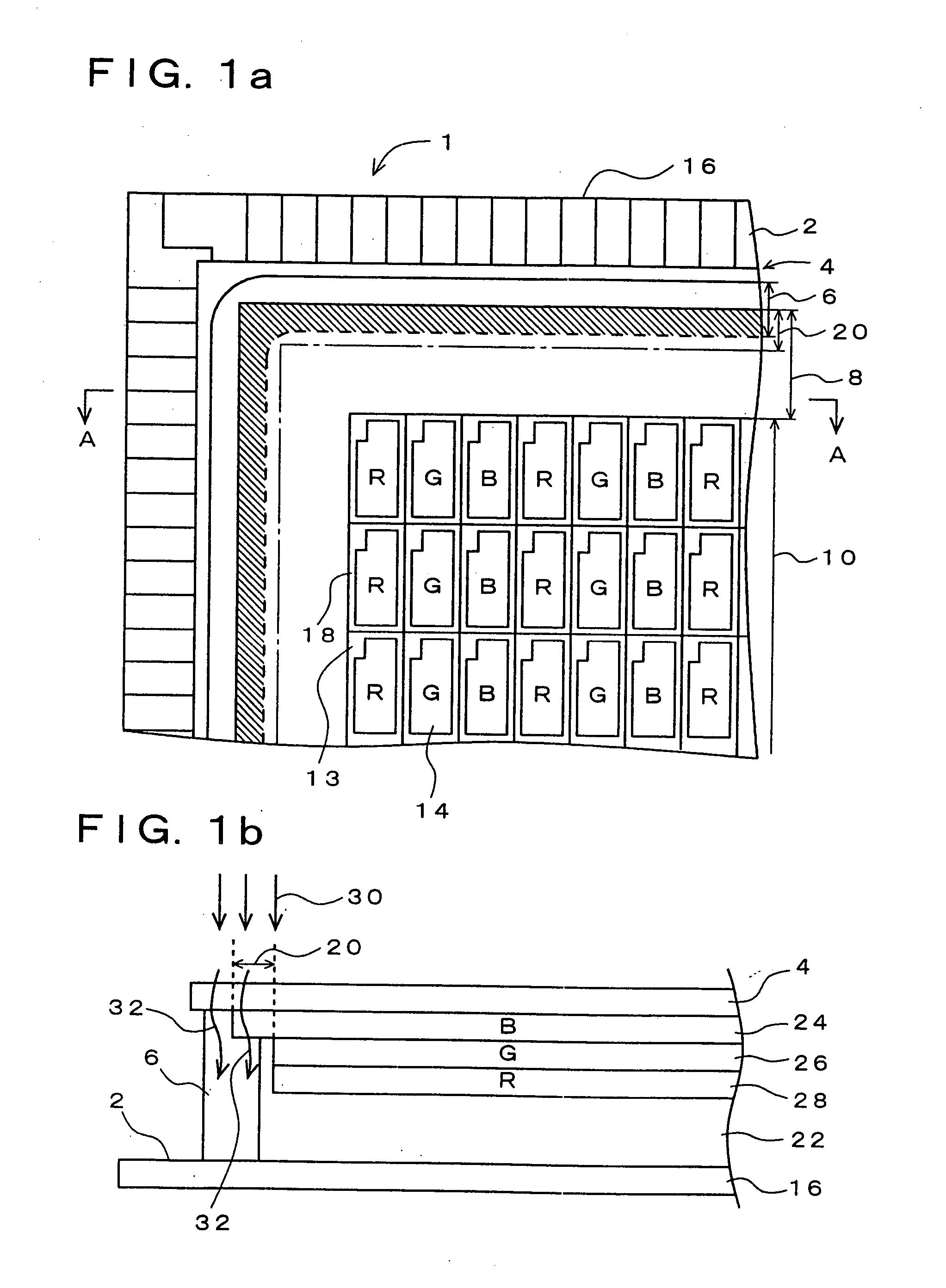
Unless a frame-shape spacer is strategically arranged, when a sealing material is spread after substrates are attached, a part of the sealing material overlaps with the end of a BM picture frame and UV light is obstructed, thereby resulting in curing defects.
Since
adhesive strength is weak in the portion of a curing defect, external stress is concentrated and peeling of a sealing material is induced.
However, by so doing, the picture-frame area is enlarged and the glass
substrate surface can not be efficiently utilized.
If a column-shape spacer equivalent to a
cell gap alone is provided in a fringe periphery of a substrate, when liquid crystal more than the amount to fill the frame-shape spacer is dropped at the time of instillation, an excess liquid crystal flows over the frame-shape spacer, uncured sealing material and liquid crystal contact, thereby dispersing contaminant.
If a liquid crystal material has strong polarity and a material for liquid crystal and a material used for an alignment
film material are inferior in electrical characteristics (i.e.
low voltage retention ratio, high
ion density, large residual
DC voltage), the “dropping mark” tends to be more visibly generated.
Specifically, although in a liquid crystal panel in which alignment control of liquid crystal of MVA-(multi-domain
vertical alignment) mode can be realized, N-type (negative
dielectric anisotropy: Δε<0) liquid crystal material and a
vertical alignment film are required,
material selection for these materials is limited in comparison with P-type liquid crystal material and a horizontal alignment film, and there are only few materials among the existing materials which satisfy requirements of electrical characteristics.
Furthermore, an instilling method has a problem in which administration to prevent substrates failed at instillation due to troubles in the process and substrates failed to create a
cell gap adjacent to a main seal from advancing to subsequent processes is difficult.
Specifically, since the
birefringence of liquid crystal viewed from the front surface of a panel when
voltage is not applies is equal to 0 in an MVA-mode liquid crystal panel, a liquid crystal layer is seen as the same as an
air layer and grasping a state of liquid crystal instillation with certainty is difficult.
However, a gap is difficult to create by a sealing material of high
viscosity and a cell gap at the edge of a seal becomes thicker then a cell gap at the center of a display, thereby resulting in generating a problem of display irregularities.
Further, upon performing an instilling method, due to variations in the environment during the period up to when a sealing material is cured by UV
irradiation after attaching substrates in a vacuum and subsequently returning the attached substrates in an
atmosphere, changes in a condition of substrates at the time of UV irradiation, and a lack of stability in positioning substrates when a gap is created or the like, a displacement in attaching or a displacement from substrate
distortion is generated, or a gap defect is generated, thereby resulting in a problem in which producing a stable product is difficult.

