Method of manufacturing semiconductor device and semiconductor device

a manufacturing method and semiconductor technology, applied in semiconductor devices, semiconductor/solid-state device details, electrical apparatus, etc., can solve the problems of increasing serious problems attributed to the time constant of interconnects, difficulty in dry etching patterning, and dual damascene methods, etc., to enhance interconnect reliability, suppress operation delays, and suppress electromigration and stress migration

Inactive Publication Date: 2006-08-24
SONY CORP
View PDF0 Cites 10 Cited by
  • Summary
  • Abstract
  • Description
  • Claims
  • Application Information

AI Technical Summary

Benefits of technology

[0041] As described above, according to the methods of manufacturing a semiconductor device and the semiconductor device obtained through any of the methods in accordance with the embodiments of the present invention, the dielectric constant of the whole interlayer and interconnect insulating films can be maintained at a low value, and thus the interconnect capacitance can be maintained at a low value. Accordingly, a high-pe

Problems solved by technology

In step with size miniaturization and increase of integration degree of semiconductor devices, delays of electrical signals attributed to the time constant of interconnects are increasingly becoming a serious problem.
The Cu, however, is difficult to pattern by dry etching unlike metal materials such as Al used in conventional multilevel interconnect structures.
In particular, a dual damascene method is attracting attention.
In addition, in high-integration semiconductor devices, an increase of interconnect capacitance causes lowering of operation speed of the semiconductor devices.
The first restriction is that the compositions of the low-k material films are close to the composition of resist used for patterning, and therefore the low-k material films are readily damaged in a resist removal process.
The second restriction is that the manufacturing process needs to have applicability to fabrication of a borderless structure, in which there is no alignment margin between interconnects and via holes.
The third restriction is that adoption of a layer with a comparatively high dielectric constant leads to an increase of interconnect capacitance.
However, when a

Method used


Image

  • Method of manufacturing semiconductor device and semiconductor device
  • Method of manufacturing semiconductor device and semiconductor device
  • Method of manufacturing semiconductor device and semiconductor device

Examples


first embodiment

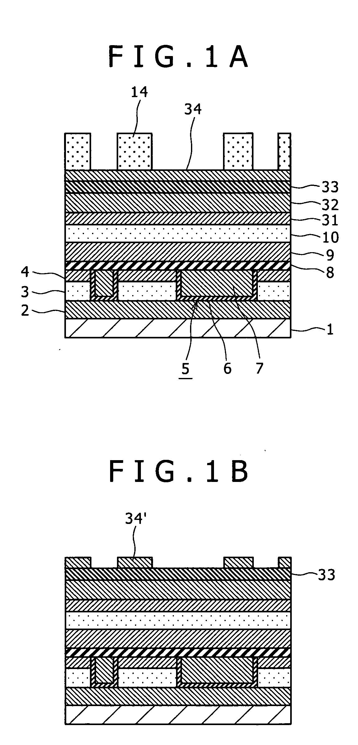
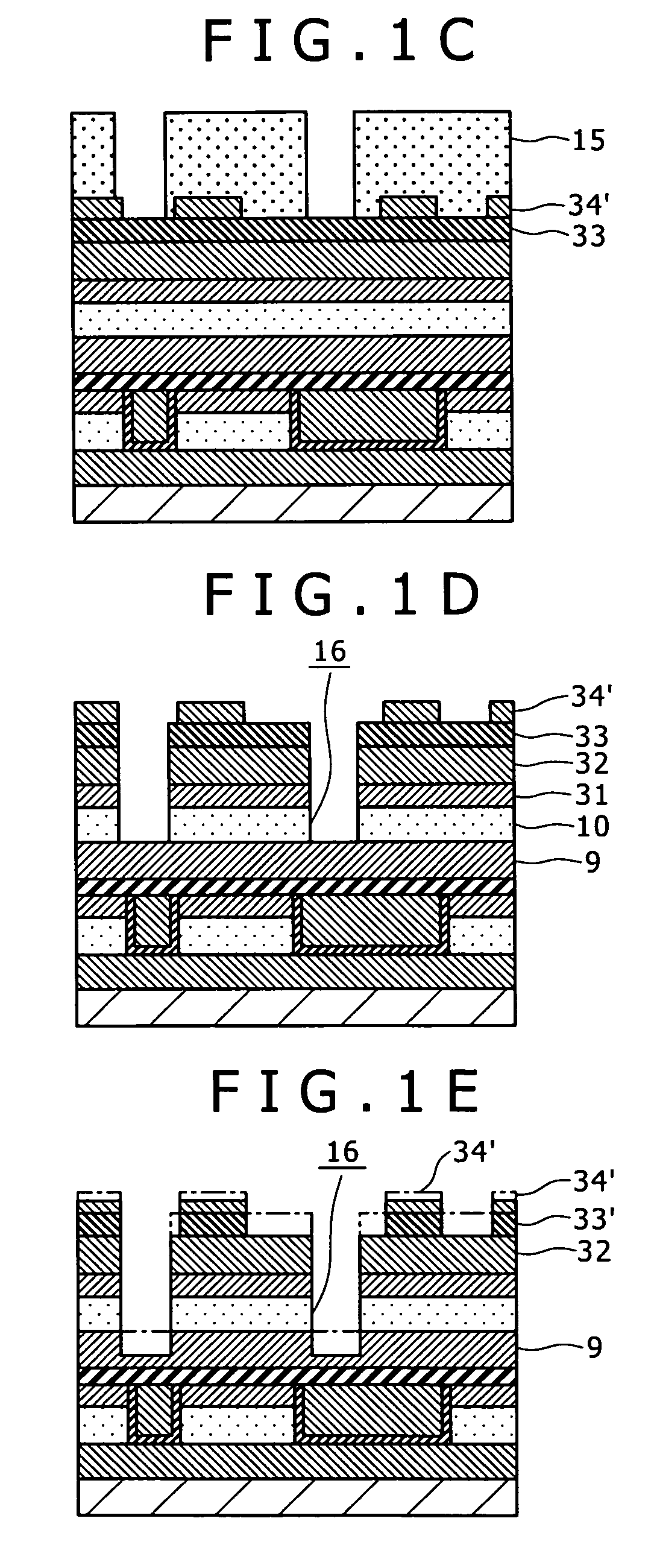
[0052] The following embodiment example shows a method of manufacturing a semiconductor device according to a first embodiment of the present invention. The first embodiment relates to the formation of a dual damascene structure by a trench-first approach, in which the formation of a mask pattern for forming interconnect trenches (interconnect trench pattern) precedes the formation of a mask pattern for forming via holes (via hole pattern). The first embodiment will be described below with reference to FIGS. 1A to 1K, which are sectional views illustrating manufacturing steps. The same elements in FIGS. 1A to 1K as those in FIG. 7A to FIG. 9 for the above-described manufacturing method as background techniques are given the same numerals.

[0053] Referring initially to FIG. 1A, over a base silicon substrate 1 having thereon element regions and so on (not shown), a multilayer film of a PAE film 3 (k=2.3) with a thickness of 90 nm and an SiOC film (MSQ) 4 (k=3.0) with a thickness of 14...

first modification

(First Modification)

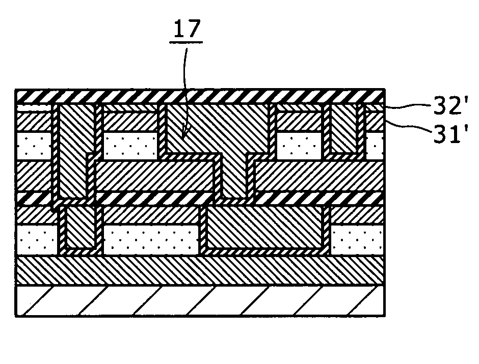
[0088] In the above description, the whole second mask 32′ is removed by CMP. Alternatively, as shown in FIG. 2, the thin-film second mask 32′ may remain on the entire first mask 31′. In this structure, the first mask 31′ serves as a third insulating film that defines the interconnect trenches 17, while the second mask 32′ serves as a fourth insulating film that also defines the interconnect trenches 17.

[0089]FIG. 3 is a graph showing the interconnect capacitance of the structure of FIG. 2 as a function of the thickness of the second mask 32′ (the fourth insulating film) that remains on the first mask 31′ (the third insulating film) with a thickness of 50 nm. In the graph, the interconnect capacitances are plotted with the thickness of the second mask 32′ being changed from 0 nm to 20 nm with an increment of 5 nm. The semiconductor device in which the thickness of the second mask 32′ (see FIG. 2) is 0 is obtained through the same method as that of the first embo...

second embodiment

[0092] A method of manufacturing a semiconductor device according to a second embodiment of the present invention will be described below with reference to FIGS. 4A to 4K, which are sectional views illustrating manufacturing steps. The same elements in the second embodiment as those in the first embodiment are given the same numerals, and detailed description thereof will be omitted.

[0093] Referring initially to FIG. 4A, in the second embodiment, the manufacturing process is advanced in the same way as the first embodiment until the step of forming Cu interconnects 7 in a PAE film 3 and an SiOC film 4 after sequential deposition of the PAE film 3 and the SiOC film 4 over a substrate 1 with the intermediary of a base insulating film 2 therebetween.

[0094] Subsequently, a first etching stopper film 8a and a second etching stopper film 8b are sequentially formed on the Cu interconnects 7 and the SiOC film 4. The first etching stopper film 8a is composed of SiC and has a thickness of 3...


PUM


Abstract

The present invention provides a method of manufacturing a semiconductor device and a semiconductor device that allow use of interlayer and interconnect insulating films having a low dielectric constant in forming a dual damascene structure. A first insulating film, a second insulating film, a first-mask forming layer, a second-mask forming layer, a third-mask forming layer, and a fourth-mask forming layer are sequentially deposited over a substrate. The fourth-mask forming layer is patterned to form a fourth mask having an interconnect trench pattern. After a resist mask is formed on the fourth mask, the layers to the second insulating film are etched to open via holes. The third-mask forming layer is etched through the fourth mask to thereby form a third mask having the interconnect trench pattern and to extend the via holes downward partway across the first insulating film. The second-mask forming layer is etched through the fourth mask to thereby form a second mask having the interconnect trench pattern, and the first insulating film that remains under the bottoms of the via holes is removed. Subsequently, the second insulating film is etched through the second mask to thereby form an interconnect trench, and then the second mask is removed.

Description

CROSS REFERENCES TO RELATED APPLICATIONS [0001] The present invention contains subject matter related to Japanese Patent Application JP 2005-035414 filed with the Japanese Patent Office on Feb. 14, 2005 and Japanese Patent Application JP 2005-361211 filed with the Japanese Patent Office on Dec. 15, 2005, the entire contents of which being incorporated herein by reference. BACKGROUND OF THE INVENTION [0002] The present invention relates to a method of manufacturing a semiconductor device and a semiconductor device, and particularly to a method of manufacturing a semiconductor device having a multilevel interconnect structure based on a dual damascene structure that has a structural shape suitable for adoption of low dielectric constant (low-k) films as interlayer insulating films and insulating films among interconnects (interconnect insulating films), and the semiconductor device. [0003] In step with size miniaturization and increase of integration degree of semiconductor devices, d...

Claims


Application Information

Patent Timeline
IPC IPC(8): H01L23/52
CPCH01L21/76808H01L21/76811H01L21/76813H01L21/76814H01L21/76829H01L21/76832H01L21/76835H01L21/76838H01L23/5226H01L23/53238H01L23/5329H01L23/53295H01L2924/0002H01L2924/00
Inventor ENOMOTO, YOSHIYUKIKAWASHIMA, HIROYUKIOKAMOTO, MASAKI
Owner SONY CORP
Why Eureka
Try Eureka