

Substrate with refractive index matching
a technology of refractive index and substrate, applied in the field of semiconductors, optical and optoelectronics, microelectronics, etc., can solve the problems of reducing reflective losses, 16% and 19% loss of light by reflection
- Summary
- Abstract
- Description
- Claims
- Application Information
AI Technical Summary
Benefits of technology
Problems solved by technology
Method used
Image

Examples
example 1
[0061] This example concerns a composite substrate comprising a thin silicon film, a transparent quartz support, and a buried antireflective layer constituted by two sub-layers. The composite substrate so produced is suitable for a component that can detect light with a wavelength centered around 500 nm.
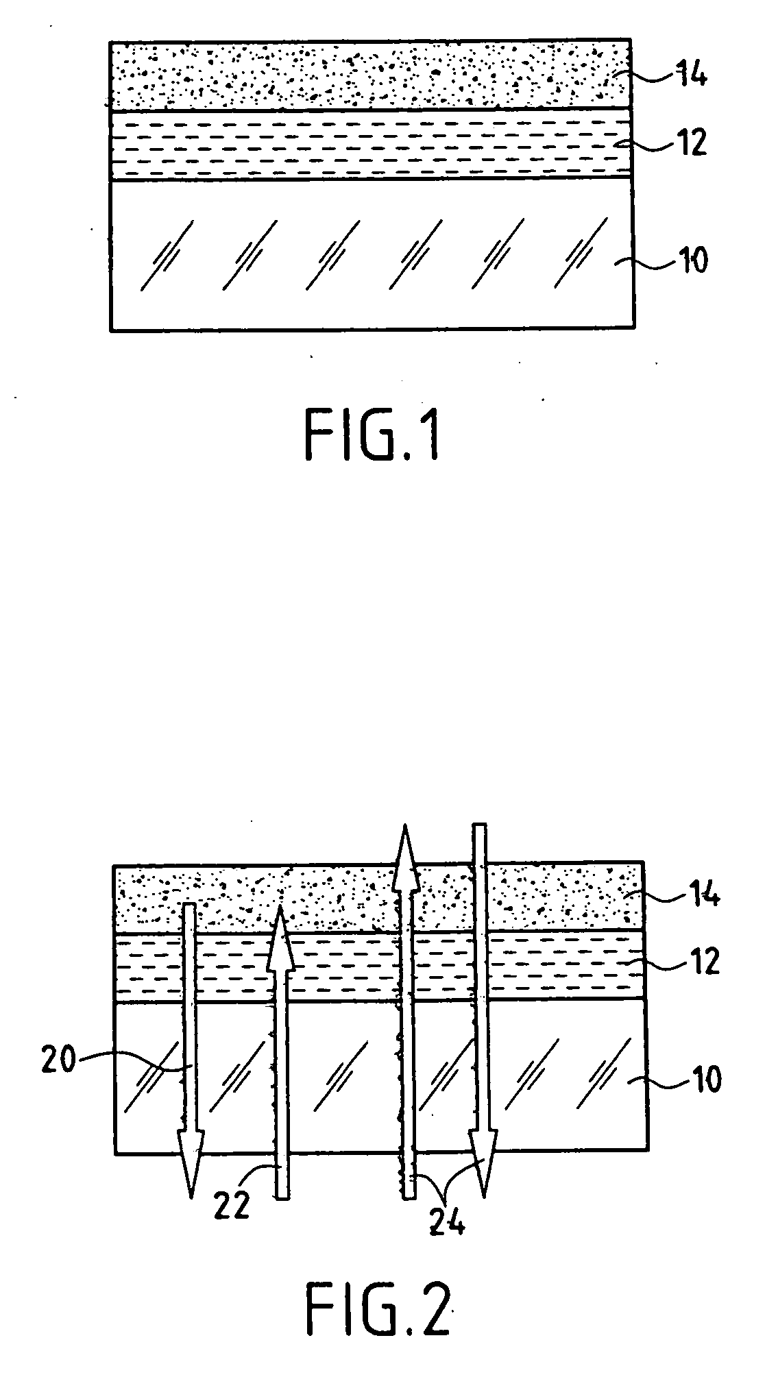
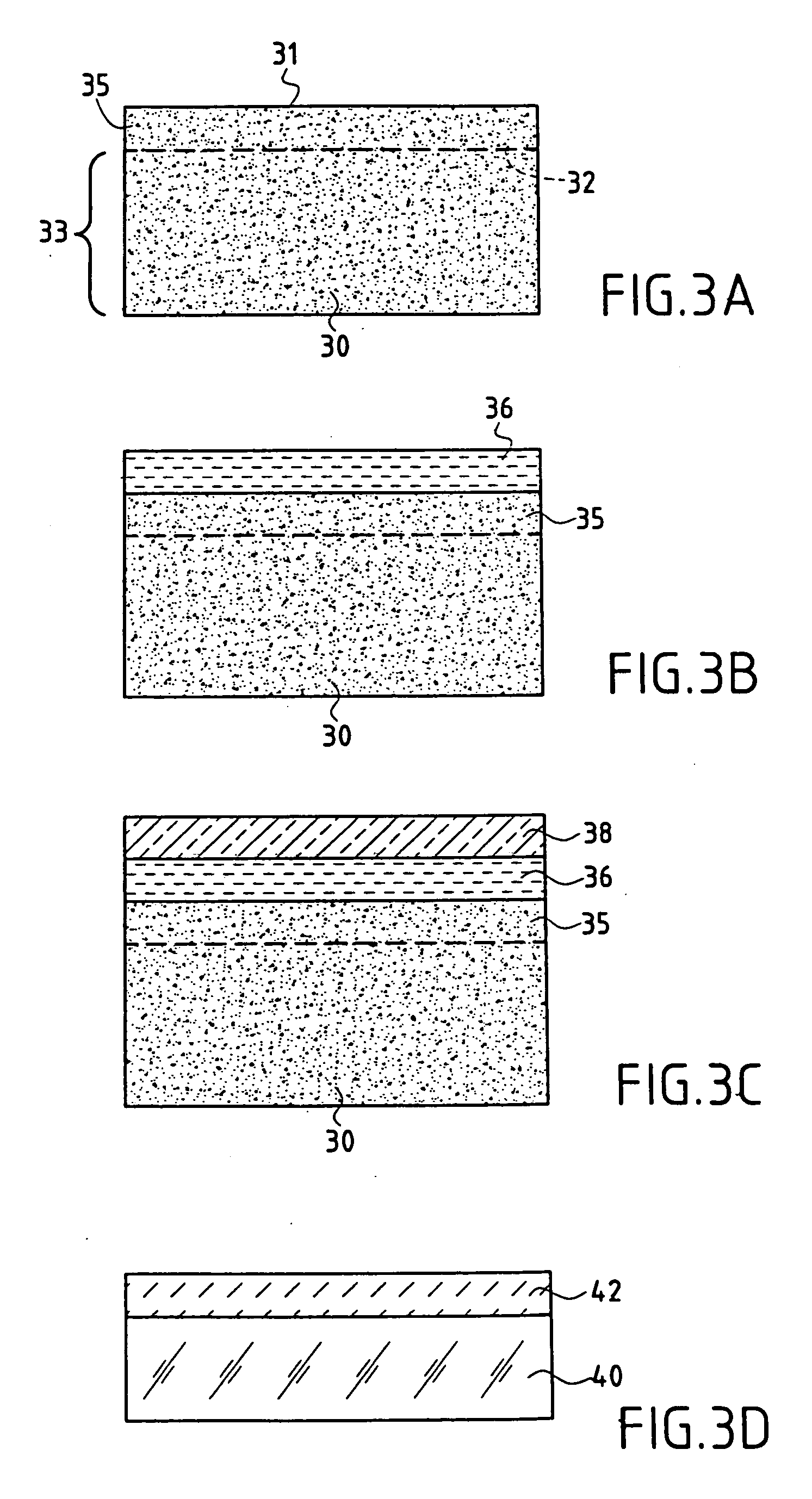
[0062] 1. Firstly (FIG. 3A), ionic implantation of hydrogen is carried out in a silicon substrate 30.
[0063] 2. A first layer 36 of the desired thickness (for example 125 nm) and constituted by amorphous silicon carbide (n˜2.6) is then applied (FIG. 3B) to the surface of implanted Si, by cathode sputtering or by chemical vapor decomposition (CVD).
[0064] 3. A second layer 38 constituted by SiOxNy (n−1.95) is applied using CVD (FIG. 3C). Polishing this deposit produces the desired thickness, for example 125 nm, and a surface that is sufficiently smooth to carry out bonding by molecular bonding.
[0065] 4. A deposit 42 of silicon oxide is then produced on the quartz support 40 (FIG. 3D...
example 2
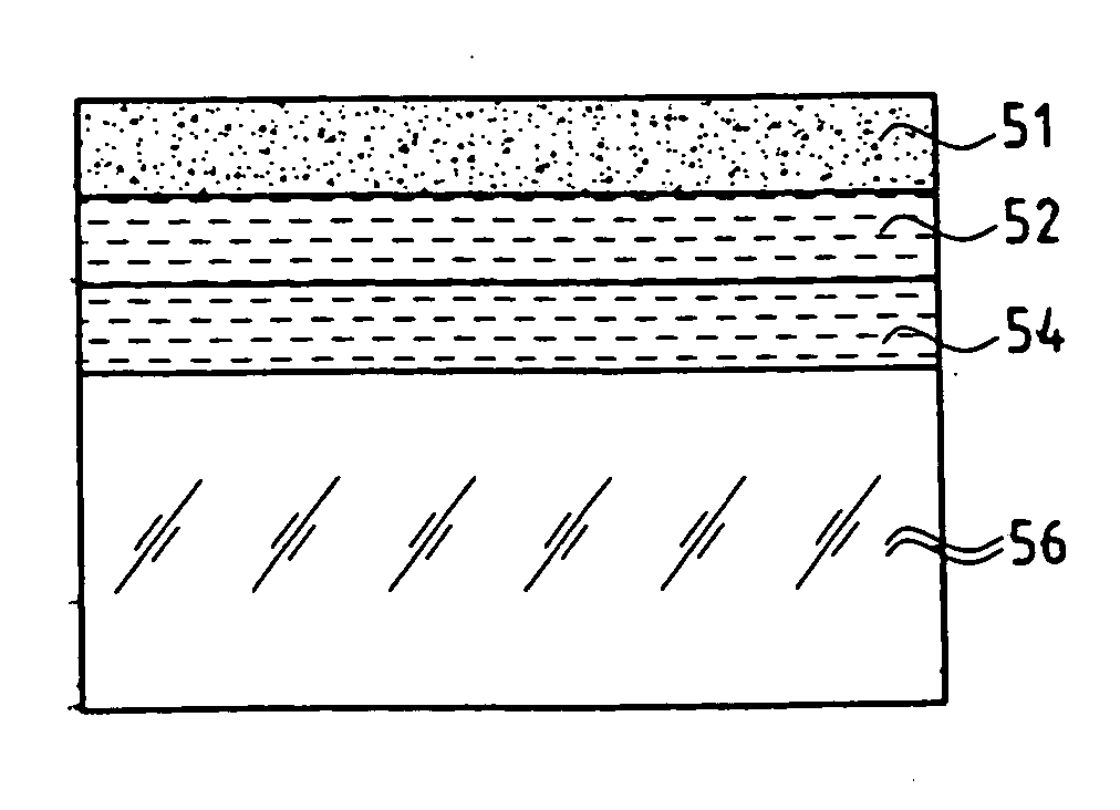
[0070] This example concerns the production of a composite substrate comprising a thin film of GaAs, a transparent glass support and a simple antireflective layer. The composite substrate so produced is suitable for an LED emitting at 640 nm:
[0071] 1. Firstly, a deposit 52 (which is optionally smoothed) of 160 nm of amorphous or polycrystalline gallium nitride (n˜2.3) is made on a monocrystalline GaAs substrate 50 which has been cleaned in advance 10 (FIG. 4A).
[0072] 2. Then a deposit 54 of SiO2, which is optionally planarized, is produced on the glass support 56 which has been cleaned in advance (FIG. 4B)
[0073] 3. After cleaning, the transparent support 56 is bonded by molecular bonding to the GaAs substrate 50 (GaN face) (FIG. 4C).
[0074] 4. Mechanical and / or chemical thinning of the GaAs substrate produces a thin film 51 of GaAs of controlled thickness (FIG. 4D).
[0075] 5. Finally, finishing is carried out on the surface of the composite substrate.
[0076] The technique for tra...
example 3
[0077] This example concerns the production of a composite substrate comprising a thin film of Si, a glass support and a simple antireflective layer. The composite substrate so produced is suitable for a solar cell. It is described in association with the same FIGS. 4A-4D:
[0078] 1. Firstly, a thin film 52 of transparent conductive oxide is applied to a substrate 50 of Si (FIG. 4A).
[0079] 2. The desired thickness is obtained by planarization of this layer (for example: 125 nm) and the surface is compatible with bonding by molecular bonding.
[0080] 3. A layer 54 of SiO2 is applied to the support 56 of glass, for bonding, and is optionally planarized.
[0081] 4. Bonding by molecular bonding is then carried out (FIG. 4C) with the transparent conductive oxide face 52 on the SiO2 face 54. Said bonding is preferably carried out at low temperature to limit diffusion of metallic elements from the conductive oxide to the silicon.
[0082] 5. Finally, mechanical and / or chemical thinning of the ...
PUM
| Property | Measurement | Unit |
|---|---|---|
| Electrical conductor | aaaaa | aaaaa |
| Antireflective | aaaaa | aaaaa |
| Transparency | aaaaa | aaaaa |
Abstract
Description
Claims
Application Information