
Deposition of permanent polymer structures for OLED fabrication

Inactive Publication Date: 2006-09-21
ROMAN PAUL J JR +1
View PDF23 Cites 14 Cited by
  • Summary
  • Abstract
  • Description
  • Claims
  • Application Information

AI Technical Summary

Benefits of technology

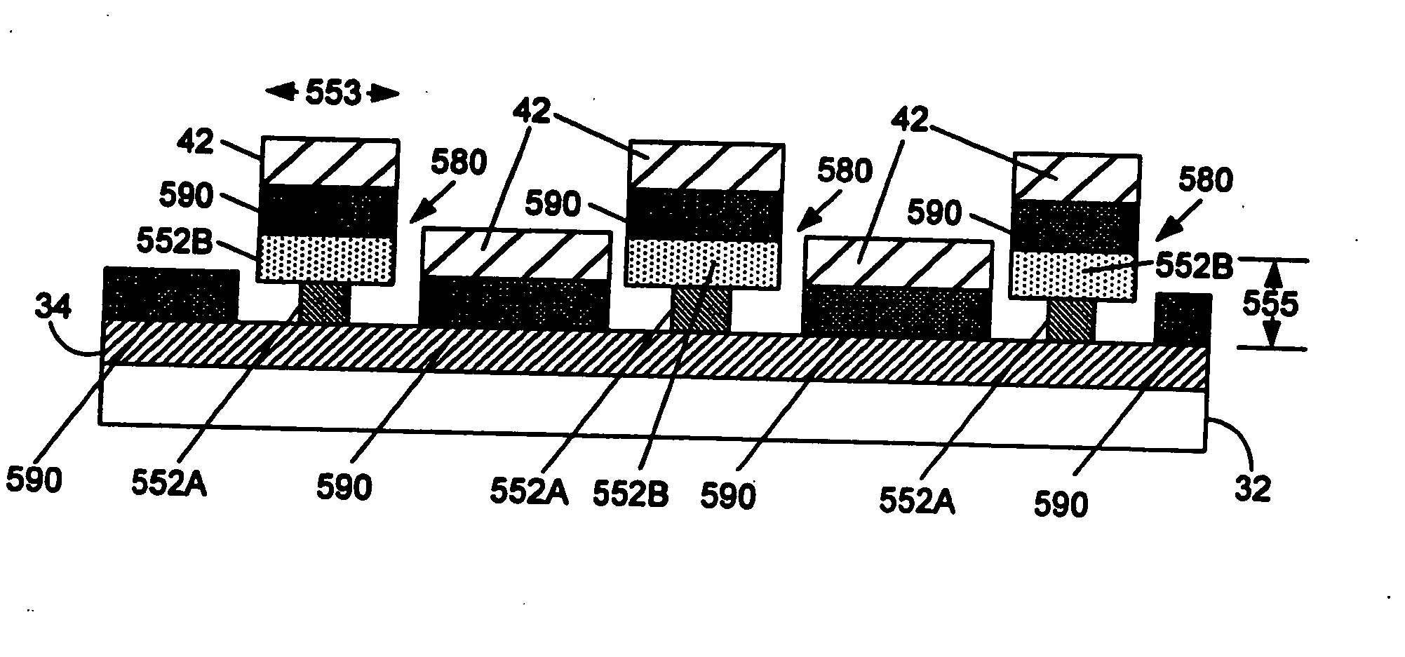
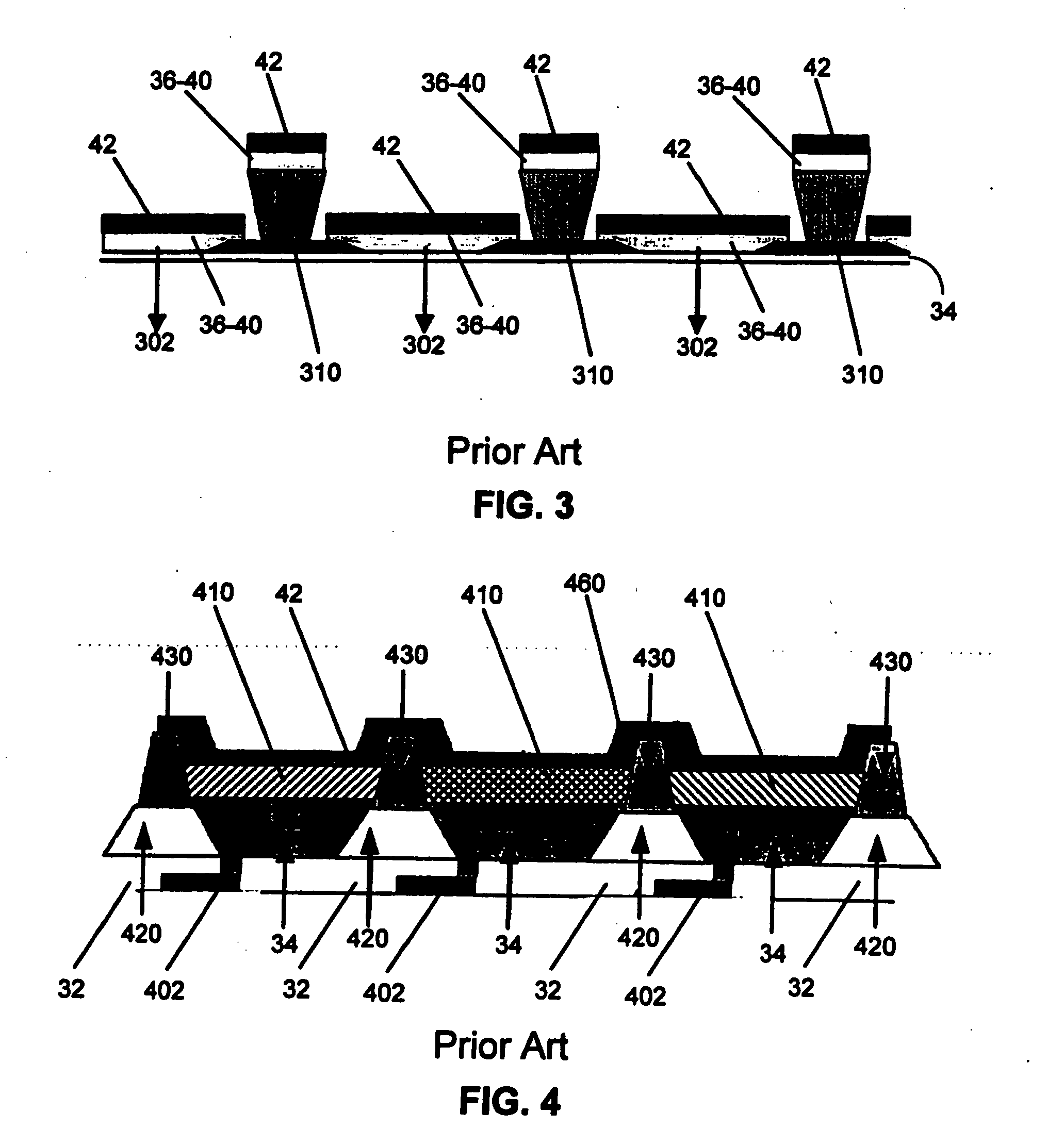
[0084] An advantage of the present invention is that feature size of structures 580 can be made smaller than the feature size of structures used to perform the same function in the prior art (e.g. undercut pillar 310 of FIG. 3). Referring to FIG. 5K, in some embodiments, undercut structures 580 have a length 553 that is between 100 nm and 500 microns and a width (not shown) that is between 100 nm and 400 microns. In some embodiments, length 553 is between 25 microns and 35 microns whereas and the width is between 15 microns and 25 microns. As referred to herein, the length 553 and width of undercut structures is measured at a top portion of the undercut structure rather than the etched undercut portion of the structure 580. In some embodiments, the thickness 555 (FIG. 5K) of structures 580 (the aggregate thickness of layers 552A and 552B) is between about 0.75 microns and about 4.5 microns. In a more preferred embodiment, the thickness 555 of structures 580 is between about 2 microns and 3 microns.
[0085] This aspect of the present invention provides novel self-aligning dual damascene type methods for making color isolation wells for color matrix OLED display applications. FIG. 7 illustrates an exemplary embodiment in accordance with this aspect of the invention. In FIG. 7A, a substrate 32 is coated with a first well layer 702.
[0086] The exact composition of first well layer 702 is application dependent. In some embodiments, the composition of the material used to form first well layer 702 is chosen such that it has good wetability properties for the predetermined emissive polymer or small molecule dye that will be deposited in the color isolation well once it has been formed. For example, in some embodiments, if the predetermined emissive polymer or small molecule dye is a hydrophobic material, the material used to make first well layer 702 is selected for its hydrophobic properties. In another example, if the predetermined emissive polymer or small molecule dye is a hydrophilic material, the material used to make first well layer 702 is selected for its hydrophilic properties. In still another example, if the predetermined emissive polymer or small molecule dye is a positively charged material, the material used to make first well layer 702 is selected for its ability to present a negatively charged surface area. Those of skill in the art will appreciate that, because the present invention does not require the use of photoresists to make color isolation wells, any material amendable to lithography can be used to make first well layer 702.
[0087] In FIG. 7B, a first precursor layer, e.g., comprising a metal complex, is applied atop first well layer 702. The first precursor layer is equivalent to layer 554 of FIG. 5D. The first precursor layer can be deposited using any of the techniques described in Step E of Section I of the present invention as well as in Section III of the present invention, below. Further, the first precursor layer can be made out of any of the materials used to make layer 554 of Section I of the present invention, above, as well as those materials described in Section III of the present invention, below. After deposition, the first precursor layer is patterned using any of the techniques described in Section I, above. Specifically, the first precursor layer is subjected to a partial conversion step in the same manner that layer 554 is subjected to such a process in Step F of Section I, above, and as illustrated in FIG. 5E. Then, the assembly is exposed to a removing means, such as the removing means described in step G of Section I, above, and as illustrated in FIG. 5F. This results in the removal of substantially unconverted precursor from the device, leaving first patterned layer 704 as illustrated in FIG. 7B. Advantageously, first patterned layer 704 serves as a hard mask in subsequent processing steps, below.
[0088] A second well layer 706 is then applied atop first patterned layer 704 and exposed portions of first well layer 702. In some embodiments, second well layer 706 is any organic-based coating that can be spun on to the assembly. In some embodiments, the material used to make second well layer 706 is the same as the material used to make first well layer 702. In other embodiments, the material used to make second well layer 706 is different then the material used to make second well layer 702. In some embodiments, the material used to make second well layer 706 is selected for its poor wetability properties. For example, in instances where the predetermined emissive polymer or small molecule dye is a hydrophobic material, the material used to make first well layer 702 is selected for its hydrophilic properties. In another example, if the predetermined emissive polymer or small molecule dye is a hydrophilic material, the material used to make first well layer 702 is selected for its hydrophobic properties. In still another example, if the predetermined emissive polymer or small molecule dye is a positively charged material, the material used to make first well layer 702 is selected for its ability to present a positively charged surface area. Without intending to be limited to any particular theory, selection of a material for second well layer 706 that is not compatible with the respective predetermined emissive polymer or small molecule dye used to fill the color isolation well serves to “trap” the emissive material at the bottom of the well, thereby alleviating containment problems that are found in the prior art.
[0089] In the step illustrated in FIG. 7C, a second precursor layer has been deposited, patterned and developed to form second patterned layer 708, as illustrated, using techniques identical to those employed in the formation of first patterned layer 704 and / or described in Steps D through Step H of Section I, above. The second precursor layer can be made out of any of the materials that can be used to make the first precursor layer.

Problems solved by technology

Attempting to perform the pattern-transfer for each step individually would be very difficult due primarily to lack of planarity of the structure resulting in alignment and depth-of-focus problems.

Method used


Image

  • Deposition of permanent polymer structures for OLED fabrication
  • Deposition of permanent polymer structures for OLED fabrication
  • Deposition of permanent polymer structures for OLED fabrication

Examples


example 1

[0108] The following example illustrates the manufacture of a color isolation well as well as an undercut pillar. The combination of a color isolation well and an undercut pillar finds application in, for example, passive matrix color-based OLED displays. The structure produced by this example is illustrated in FIG. 8. Spin TOK OFPR 800-20 photoresist is coated on a silicon substrate using a CEE Model 100CB manual spin coater at a speed of 5000 rpm, for 20 seconds. The photoresist is baked on a hotplate at 230° C. for 1 minute. Next, precursor is spin coated on the device using a CEE spin coater at a speed of 5000 rpm for a period of 20 seconds. The precursor is exposed using an OAI deep ultraviolet contact aligner for a period of fifteen minutes with a power of 1.8 mJ / cm2. The precursor is then spin developed by a twenty second application of methyl isobutyl ketone:hexane:hexane (1:10) using a CEE spin coater at a speed of 500 rpm. Next, the precursor is post-developed using an ult...

example 2

[0109] The following example illustrates the manufacture of the undercut pillar illustrated in FIG. 6. A MicroChem XP LOR 10B (polyimide based lift-off layer) is spin coated onto a silicon substrate using a CEE Model 100CB manual spin coater at a speed of 5000 rpm for a period of 20 seconds. The LOR is baked on a hotplate at 230° C. for five minutes. Then, TOK OFPR 800-20 is spin coated onto the device using a CEE spin coater at a speed of 5000 rpm for a period of 20 seconds. The photoresist is baked on a hotplate at a temperature of 230° C. for one minute before precursor is spin coated onto the device using a CEE spin coater at a speed of 5000 rpm for 20 seconds. The precursor is exposed using an OAI deep ultraviolet contact aligner for a period of fifteen minutes with a power of 1.8 mJ / cm2. Next the precursor is spin developed by a twenty second application of methyl isobutyl ketone:hexane:hexane (1:10) using a CEE spin coater at a speed of 500 rpm. Next, the device is reactive i...

example 3

[0110] This example provides a general process for photochemical metal organic deposition (PMOD)-based fabrication of permanent polymer structures such as those described in Sections I and II of the present invention. First, the photochemical metal organic precursor compound(s) are isolate, and purified as necessary. Any of the materials disclosed in Section III of the invention, for example, can be used. Next, the photochemical metal organic precursor formulation is prepared by dissolving the isolated (and possibly purified) metal-organic precursor compound(s) in solvents appropriate for coating. The substrate (or temporary substrate) is coated with a pattern-transfer layer. The pattern-transfer layer is a material that will become the permanent polymer structure. The solvate metal-organic precursor formulation is then overlayed on the pattern-transfer layer and selectively exposed to ultraviolet radiation (at ambient or elevated temperature) initiating a photochemical reaction whe...


PUM


Abstract

A light emitting display comprising a first electrode layer on a substrate. The electrode layer is patterned to form a plurality of laterally spaced apart strips in a first direction. A plurality of spacedly disposed light emitting organic elements with a second electrode layer atop are disposed on the first electrode layer in a second direction. An undercut structure made of an undercut pattern transfer layer and an overlaying pattern transfer layer. The undercut structure is disposed between the plurality of spacedly disposed light emitting organic elements. A light emitting display having a color isolation well. The color isolation well is characterized by a first well layer and a second well layer in which the first well layer matches a property of an emissive polymer or small molecule dye held by the well whereas the second well layer does not match the property.

Description

CROSS-REFERENCE TO RELATED APPLICATIONS [0001] This application is a continuation of Ser. No. 10 / 422,212, filed Apr. 23, 2003 which is a continuation-in-part of co-pending application Ser. No. 09 / 875,115 to Maloney, et al., published as US 2002 / 0076495, that was filed Jun. 6, 2001 and is entitled “Method of Making Electronic Materials,” which is hereby incorporated by reference in its entirety.FIELD OF THE INVENTION [0002] The present invention relates to improved organic electroluminescent devices and improved methods for manufacturing organic electroluminescent devices. Organic electroluminescent devices include organic light-emitting diodes and polymer light-emitting diodes. They are used in a number of devices, such as car radios, mobile phones, digital cameras, camcorders, personal digital assistants, and other devices using flexible and non-flexible displays. BACKGROUND OF THE INVENTION [0003] Over the past two decades, new flat panel display technology based on light emission...

Claims


Application Information

Patent Timeline
IPC IPC(8): H05B33/00H01L51/50B05D3/00B05D5/12G03F7/004H01L21/00H01L21/027H01L21/033H01L21/06H01L21/308H01L21/31H01L21/469H01L27/15H01L27/32H01L35/24H01L51/40H01L51/56
CPCG03F7/0042H01L21/0271H01L21/0332H01L21/0337H01L21/0338H01L21/3081H01L21/3086H01L21/3088H01L21/76807H01L21/76811H01L21/76813H01L27/3211H01L27/3246H01L27/3283H01L51/56H10K59/35H10K59/122H10K59/173H10K71/40H10K71/231H10K71/00
Inventor ROMAN,, PAUL J. JR.MADSEN, HAROLD O.
Owner ROMAN PAUL J JR
Learn More