
Porous underlayer film and underlayer film forming composition used for forming the same

Inactive Publication Date: 2006-09-21
NISSAN CHEM IND LTD
View PDF8 Cites 29 Cited by
  • Summary
  • Abstract
  • Description
  • Claims
  • Application Information

AI Technical Summary

Benefits of technology

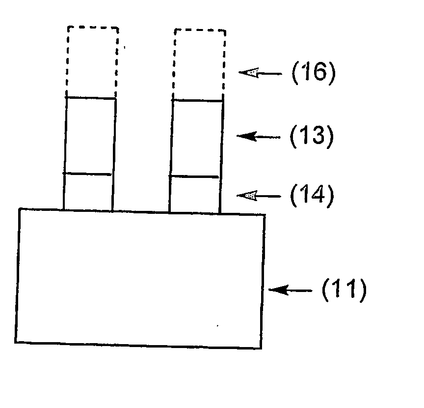
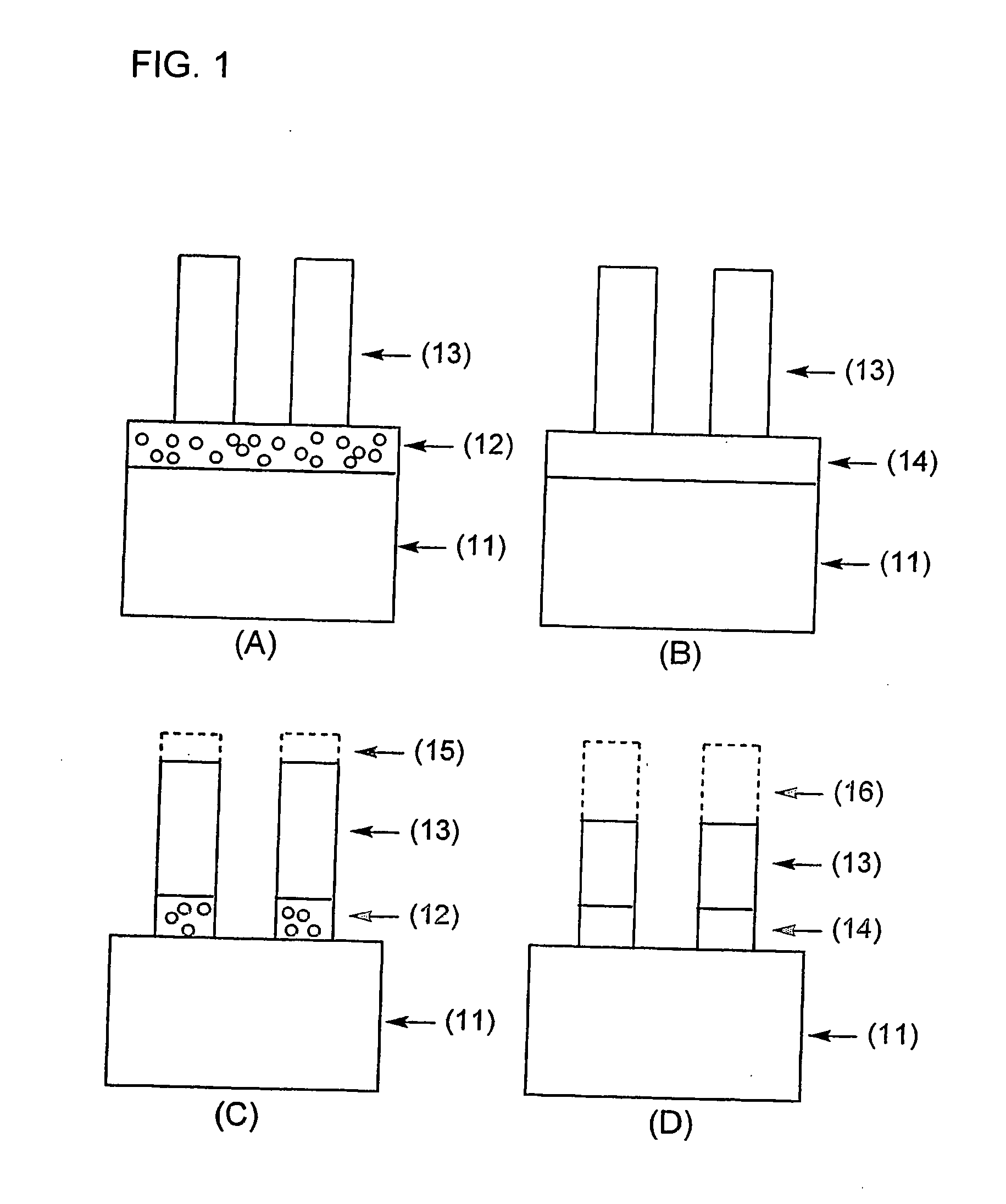
[0026] The present invention having the above-mentioned constituents makes possible to provide a porous underlayer coating causing no intermixing with photoresists and having a high dry etching rate.
[0027] The resulting porous underlayer coating can be rapidly removed in dry etching process. Therefore, reduction in film thickness of photoresist acting as a protective coating in the processing of semiconductor substrate can be suppressed.
[0028] In addition, the method according to the present invention makes possible to secure a protective coating composed of a patterned photoresist and underlayer coating, which is required for the processing of semiconductor substrate, even when the initial film thickness of photoresist is small.

Problems solved by technology

Along with this change, influences of random reflection and standing wave of a substrate have become serious problems.
However, it is difficult to apply organic material for anti-reflective coating on a substrate having a high aspect ratio, and in recent years, material with particular emphasis on filling property or flattening property has been developed (see, for example JP 2000-294504 A, JP 200247430 A, JP 2002-190519 A and WO 02 / 05035 pamphlet).
In addition, if it takes a long time to remove the underlayer coating, the reduced amount of the photoresist becomes large, and this causes a problem that the photoresist cannot maintain a film thickness required for the processing of substrates.

Method used


Image

  • Porous underlayer film and underlayer film forming composition used for forming the same
  • Porous underlayer film and underlayer film forming composition used for forming the same
  • Porous underlayer film and underlayer film forming composition used for forming the same

Examples


synthetic example 1

[0103] In 27.91 g of propylene glycol monomethyl ether, 20.93 g of 2-hydroxypropyl methacrylate and 6.98 g of benzyl methacrylate were dissolved, and nitrogen was flowed to the reaction solution for 30 minutes, then the temperature was raised to 70° C. While the reaction solution was maintained at 70° C., 0.3 g of azobisisobutyronitrile was added. Then, the solution was stirred under nitrogen atmosphere at 70° C. for 24 hours to obtain a solution of a copolymer of 2-hydroxypropyl methacrylate with benzyl methacrylate. GPC analysis of the resulting polymer showed that it had a weight average molecular weight of 15000 in terms of standard polystyrene.

synthetic example 2

[0104] In 30 g of ethyl lactate, 30 g of 2-hydroxyethyl acrylate was dissolved, and nitrogen was flowed to the reaction solution for 30 minutes, then the temperature was raised to 70° C. While the reaction solution was maintained at 70° C., 0.3 g of azobisisobutyronitrile was added. Then, the solution was stirred under nitrogen atmosphere at 70° C. for 24 hours to obtain a solution of poly(2-hydroxyethyl)acrylate. GPC analysis of the resulting polymer showed that it had a weight average molecular weight of 9800 in terms of standard polystyrene.

example 1

[0105] To 10 g of a solution containing 5 g of the polymer obtained in Synthesis Example 1, 1.15 g of hexamethoxy methyl melamine, 0.012 g of pyridinium-p-toluenesulfonic acid, 0.77 g of propylene glycol monomethyl ether and 8.66 g of dimethylsulfoxide were added to obtain 30% solution. Then, 0.309 g (5% in solid content) of blowing agent: 4,4-oxybisbenzene sulfonyl hydrazide was added thereto. Thereafter, the resulting solution was filtered through a micro filter made of polyethylene having a pore diameter of 0.20 μm to prepare an underlayer coating forming composition solution.


PUM


Abstract

There is provided an underlayer coating causing no intermixing with photoresist layer and having a high dry etching rate compared with photoresist, which is used in lithography process of manufacture of semiconductor device. Concretely, it is an underlayer coating forming composition for forming a porous underlayer coating for use in manufacture of semiconductor device, comprising a blowing agent, an organic material and a solvent, or a polymer having a blowing group and a solvent. The underlayer coating formed from the composition has porous structure which has pores therein, and makes possible to attain a high dry etching rate.

Description

TECHNICAL FIELD [0001] The present invention relates to a method for forming photoresist pattern for use in manufacture of semiconductor device, including a step of forming a porous underlayer coating between a semiconductor substrate and a photoresist. In addition, the present invention relates to an underlayer coating forming composition for forming a porous underlayer coating used in the formation of a photoresist pattern for use in manufacture of semiconductor device, and to a method for forming a porous underlayer coating by using the underlayer coating forming composition, and a porous underlayer coating formed form the underlayer coating forming composition. BACKGROUND ART [0002] Conventionally, in the manufacture of semiconductor devices, micro-processing by lithography using a photoresist has been carried out. The micro-processing is a processing method comprising forming a thin film of a photoresist on a semiconductor substrate such as a silicon wafer, irradiating actinic ...

Claims


Application Information

Patent Timeline
IPC IPC(8): H01L21/302H01L21/461G03F7/11
CPCG03F7/11
Inventor TAKEI, SATOSHISAKAIDA, YASUSHI
Owner NISSAN CHEM IND LTD
Learn More