Device for generating or detecting electromagnetic radiation, and fabrication method of the same

Inactive Publication Date: 2006-09-28
CANON KK
View PDF22 Cites 66 Cited by
  • Summary
  • Abstract
  • Description
  • Claims
  • Application Information

AI Technical Summary

Benefits of technology

[0009] It is an object of the present invention to provide a device for generating or detecting electromagnetic radiation, which is capable of relati

Problems solved by technology

In those methods of converting light into THz radiation, however, output power typically cannot be increased and power consumption typically cannot be decreased, since converting efficiencies are low.
However, the device of

Method used


Image

  • Device for generating or detecting electromagnetic radiation, and fabrication method of the same
  • Device for generating or detecting electromagnetic radiation, and fabrication method of the same
  • Device for generating or detecting electromagnetic radiation, and fabrication method of the same

Examples


first embodiment

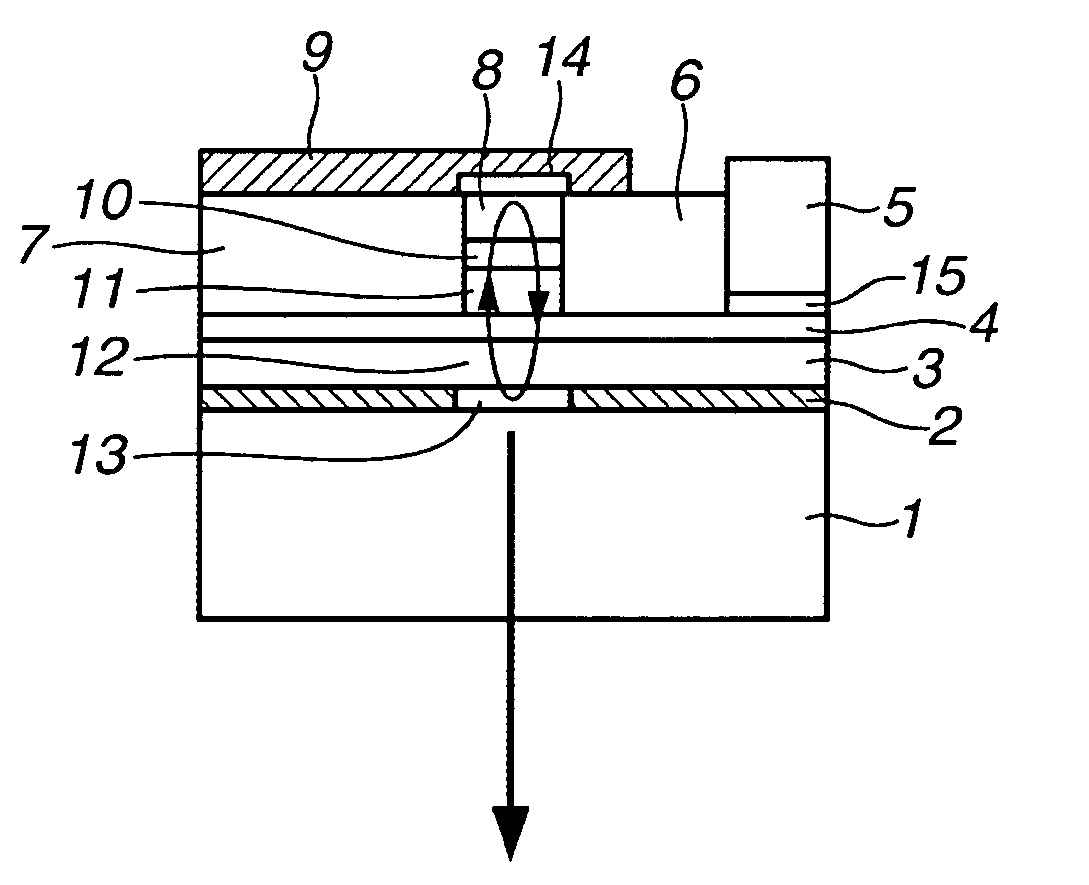
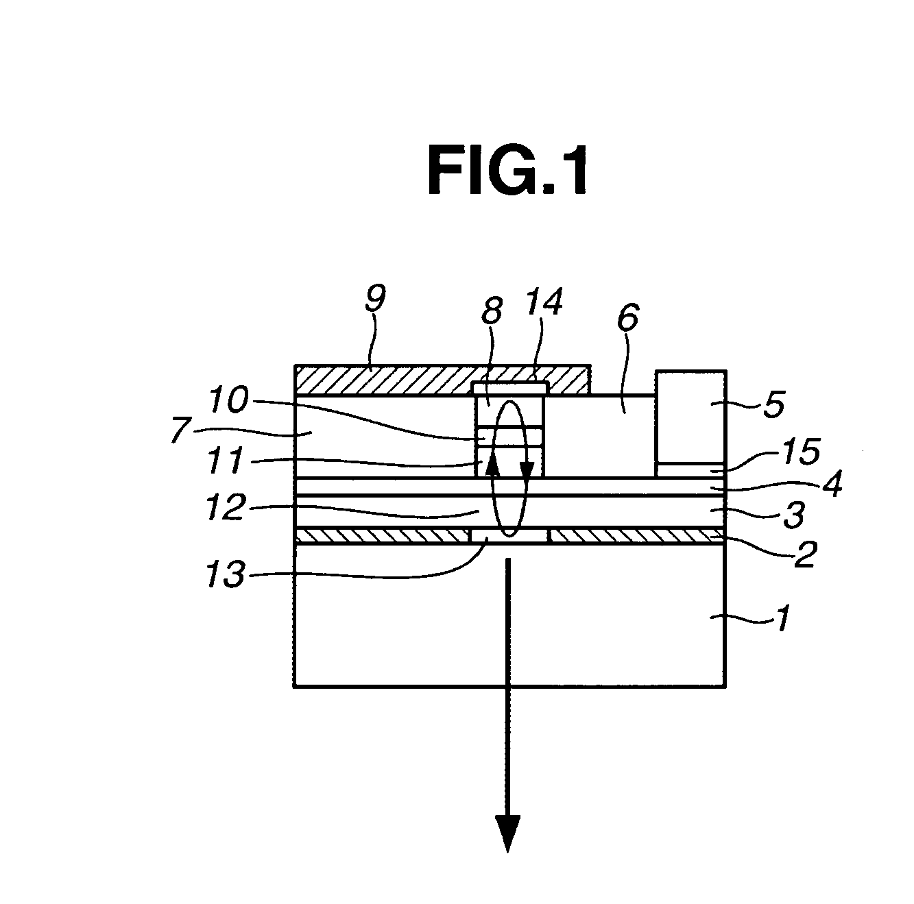
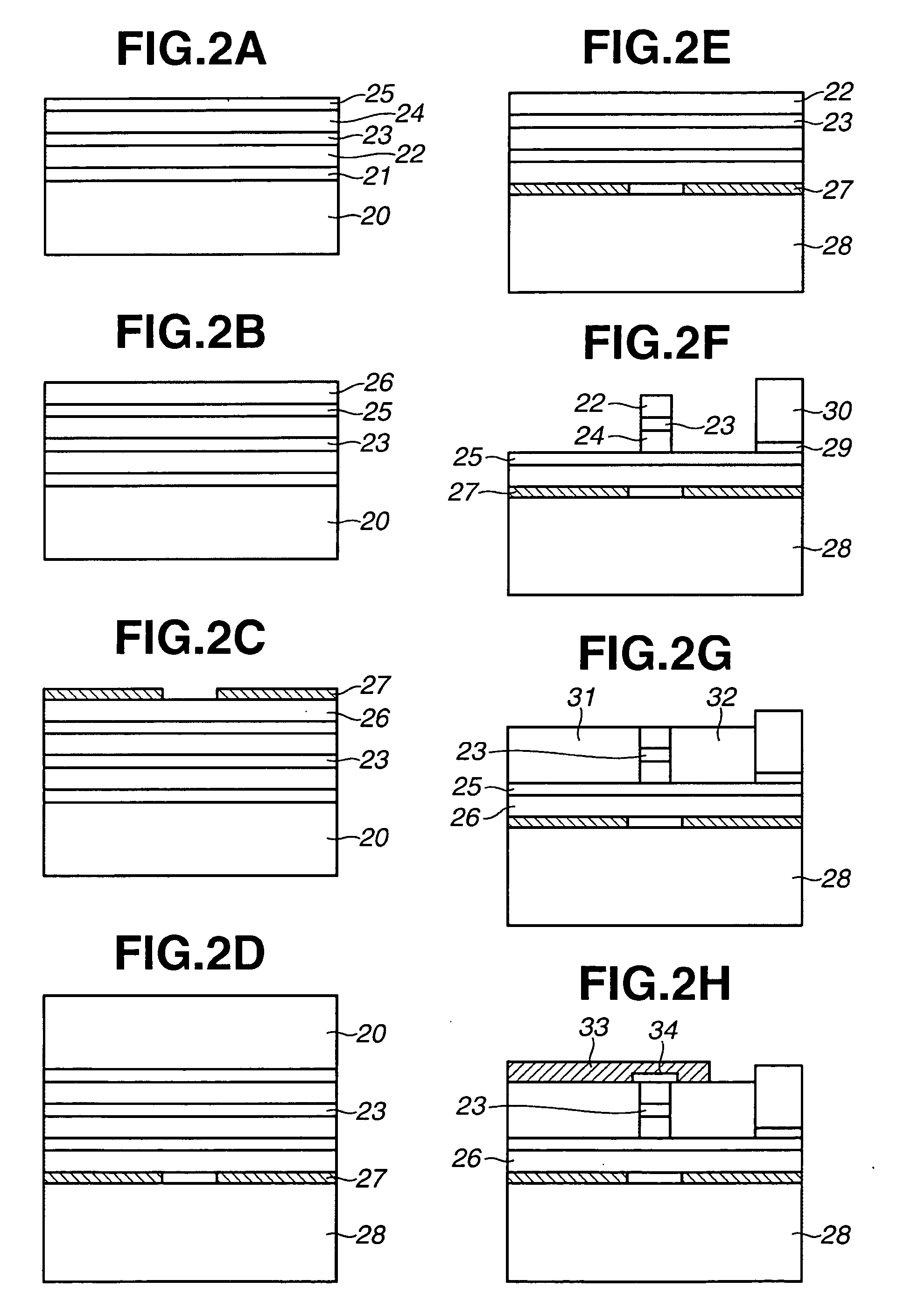
[0029] A fabrication process of the first embodiment will be described with reference to FIGS. 2A to 2H.

[0030] As illustrated in FIG. 2A, an InP buffer layer 21, an InGaAs contact layer 22, an active layer 23 with the above-discussed InAlAs / InGaAs multi-layer structure, an InGaAs contact layer 24, and a heavily-doped InGaAs contact layer 25 are grown on an InP substrate 20 in an epitaxial manner using molecular beam epitaxy (MBE) or the like.

[0031] Then, as illustrated in FIG. 2B, an undoped Si spacer layer 26 is formed using chemical vapor deposition (CVD) or the like. An Au thin film 27 for the metallic mirror is then formed, and an opening for transmitting electromagnetic radiation therethrough is formed in the Au thin film 27, as illustrated in FIG. 2C.

[0032] After that, as illustrated in FIG. 2D, the wafer is bonded to a high resistivity Si substrate 28 with the metallic mirror 27 being used as a bonding face. Here, it is possible to employ a bonding method of using a resin a...

second embodiment

[0044] In the second embodiment, a Fresnel lens 37 for converging an emitted radiation beam is formed on a radiation emerging surface of the substrate 38, using etching or the like. In place of the Fresnel lens 37, an external lens can be used. This also holds true in other embodiments.

[0045] When the above dielectric multi-layer mirror is employed, there is no need to form an opening for transmitting electromagnetic radiation therethrough. Further, the reflectivity of the mirror can be regulated over a wide range by selecting materials and the number of layers in the multi-layer mirror. Therefore, the structure can be flexibly determined depending on the type of the device, i.e., a low threshold type or a high output type. For example, the low threshold type can be achieved when the number of layers is increased to enhance the reflectivity. Alternatively, the high output type can be achieved when the reflectivity on the radiation emitting side is reduced. The second embodiment is s...

fourth embodiment

[0049] In other words, the device of the fourth embodiment includes a substrate 50, a metallic mirror layer 51 with a plurality of openings, a spacer layer 52, an Si-high-doped InGaAs layer 53, Si-doped n-type InGaAs contact layers 57 and 59, active layers 58 with a quantum well structure having a semiconductor heterostructure, and burying layers 55. The active layer 58 generates a gain for electromagnetic radiation due to transition between subbands created in quantum wells in the quantum well structure. When the respective devices are provided at intervals of less than about 100 microns that is the oscillation wavelength, electromagnetic radiation is oscillated from the respective devices with a common-phase relationship maintained therebetween. Therefore, respective electromagnetic radiation waves interfere with each other so that a single beam of electromagnetic radiation can be emitted.

[0050] In the above structure, it is possible to cause oscillation and emission of electromag...


PUM


Abstract

A device for generating or detecting electromagnetic radiation includes a substrate, a gain medium provided on the substrate, a plurality of reflectors for confining electromagnetic radiation at a predetermined frequency range and substantially perpendicular to a face of the substrate, and spacer means for spacing the reflectors from each other at a predetermined distance, with the gain medium being sandwiched between the reflectors. The gain medium has a quantum well structure formed of a semiconductor material, and gives a gain to electromagnetic radiation by transitioning between subbands created in at least a quantum well in the quantum well structure. The spacer means is formed of a material different from a material of the gain medium.

Description

BACKGROUND OF THE INVENTION [0001] 1. Field of the Invention [0002] The present invention relates to a device for generating or detecting electromagnetic radiation, such as terahertz (THz) electromagnetic radiation, and a use and fabrication method for such a device. In this specification, the terminology “the terahertz (THz) electromagnetic radiation” or “terahertz (THz) radiation” or “terahertz (THz)” is used for electromagnetic radiation in a frequency range between about 30 GHz and about 30 THz. [0003] 2. Description of the Related Background-Art [0004] In recent years, non-destructive sensing techniques have been developed using terahertz (THz) radiation. As applications of electromagnetic radiation in the above frequency range, there have been developed imaging techniques for achieving a perspective inspection apparatus capable of being safely used in place of an X-ray imaging apparatus, spectroscopy techniques for acquiring |absorption spectrum and complex dielectric constant...

Claims


Application Information

Patent Timeline
IPC IPC(8): H01L33/00B82Y15/00B82Y20/00G01N21/35G01N21/3581H01L31/10H01S1/02H01S5/183H01S5/343
CPCB82Y20/00G01N21/3581H01L31/0232H01L31/03046H01L31/035236H01S1/02H01S5/18305H01S5/18308H01S5/18388H01S5/2213H01S5/2275H01S5/3401H01S2302/02Y02E10/544
Inventor OUCHI, TOSHIHIKOSEKIGUCHI, RYOTA
Owner CANON KK
Why Eureka
Try Eureka