MOSFET structure with ultra-low K spacer

a mosfet and ultra-low k spacer technology, applied in the field of mosfet structure with ultra-low k spacer, can solve the problems of significant parasitic capacitance between the gate conductor and the source and drain extension, mosfet switching speed, and degrade the performance of mosfet in alternating current (ac) applications, so as to suppress parasitic overlap capacitance

Inactive Publication Date: 2006-10-05
GOOGLE LLC
View PDF24 Cites 55 Cited by
  • Summary
  • Abstract
  • Description
  • Claims
  • Application Information

AI Technical Summary

Benefits of technology

[0013] Therefore, the embodiments of the field effect transistor structure and method of forming the structure described above incorporates a multi-layer sidewall spacer. In one embodiment, the multi-layer sidewall spacer comprises gap layer with a permittivity value of one adjacent to the gate and a permeable low-K dielectric layer with a permittivity of value of less than three adjacent to the gap layer. In another embodiment, the multi-layer sidewall spacer comprises a first L-shape dielectric layer with a permittivity value of less than three and a second dielectric layer. These multi-layer sidewall spacers of the transistor structures suppress parasitic overlap capacitance between the gate conductor and the source and drain extensions that extend beneath the gate conductor and gate oxide layer without degrading drive current and effecting overall MOSFET performance. These, and other, aspects and objects of the invention will be better appreciated and understood when considered in conjunction with the following description and the accompanying drawings. It should be understood, however, that the following description, while indicating embodiments of the present invention and numerous specific details thereof, is given by way of illustration and not of limitation. Many changes and modifications may be made within the scope of the present invention without departing from the spirit thereof, and the invention includes all such modifications.

Problems solved by technology

However, in MOSFET structures in which the gate oxide also overlaps the source and drain extensions, a significant parasitic capacitance is created between the gate conductor and the source and drain extensions.
This parasitic capacitance can significantly reduce the MOSFET switching speed and, thereby, can degrade the performance of the MOSFET in alternating current (AC) applications.

Method used


Image

  • MOSFET structure with ultra-low K spacer
  • MOSFET structure with ultra-low K spacer
  • MOSFET structure with ultra-low K spacer

Examples


Embodiment Construction

[0031] The present invention and the various features and advantageous details thereof are explained more fully with reference to the non-limiting embodiments that are illustrated in the accompanying drawings and detailed in the following description. It should be noted that the features illustrated in the drawings are not necessarily drawn to scale. Descriptions of well-known components and processing techniques are omitted so as to not unnecessarily obscure the present invention. The examples used herein are intended merely to facilitate an understanding of ways in which the invention may be practiced and to further enable those of skill in the art to practice the invention. Accordingly, the examples should not be construed as limiting the scope of the invention.

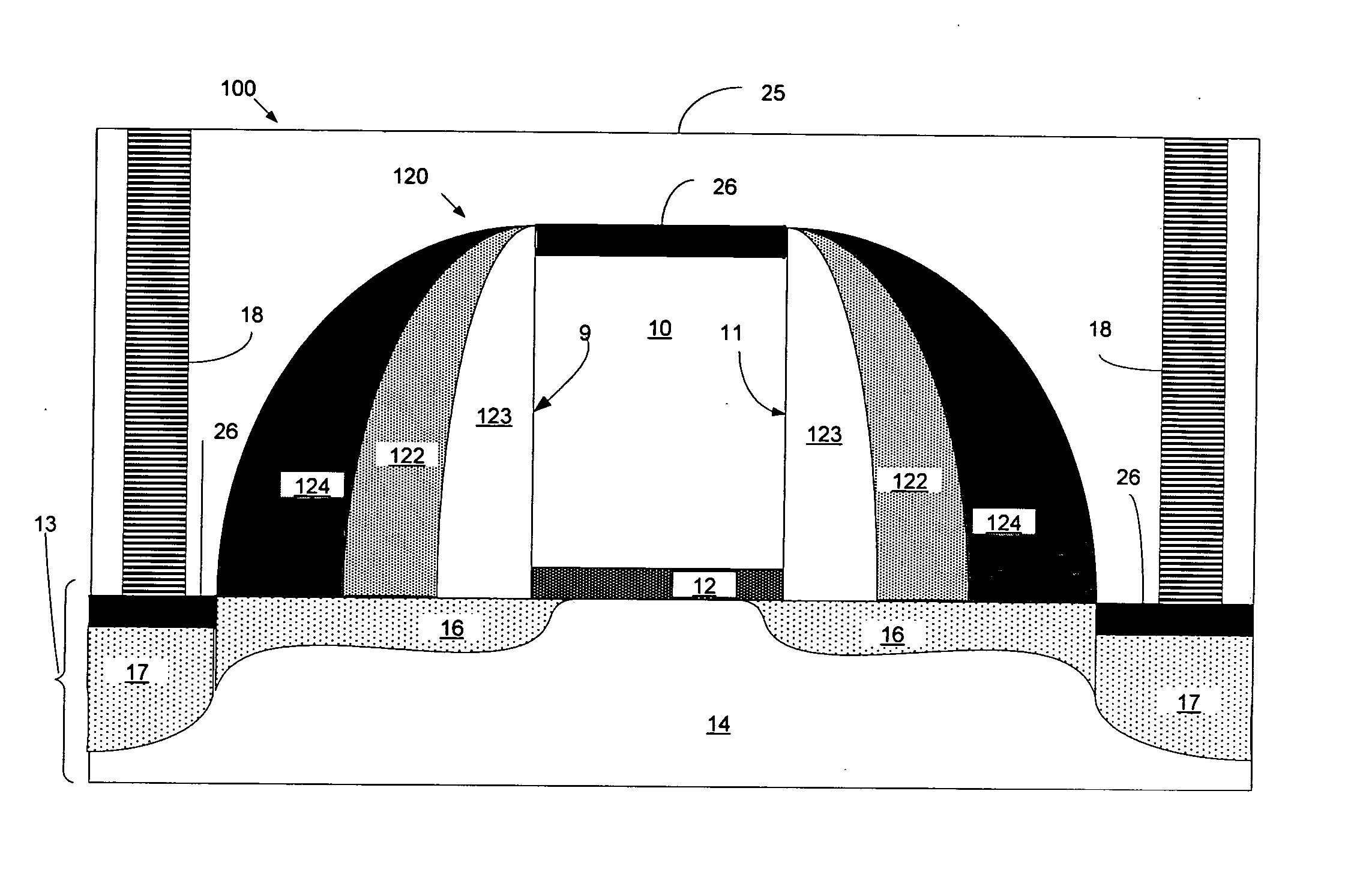
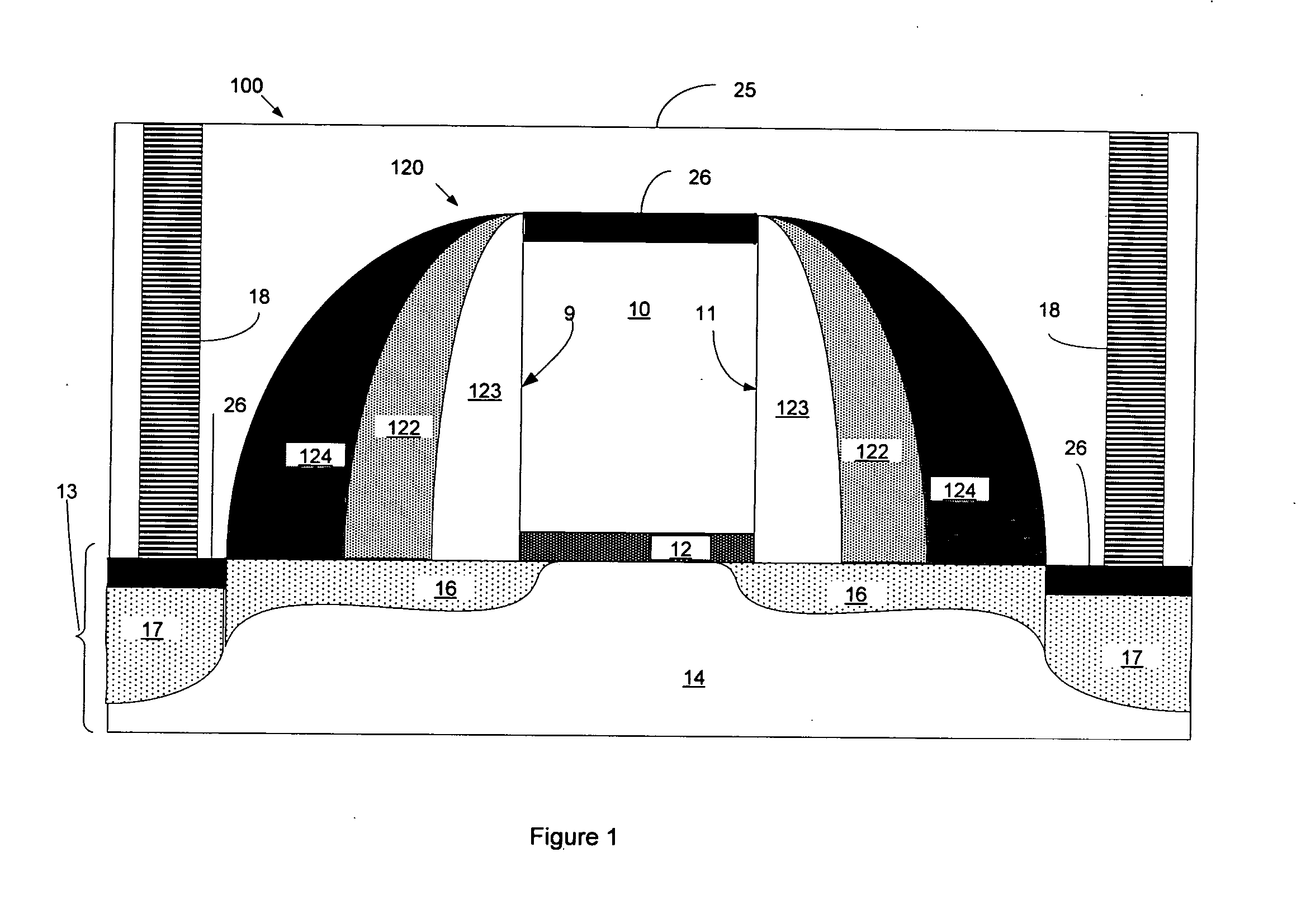
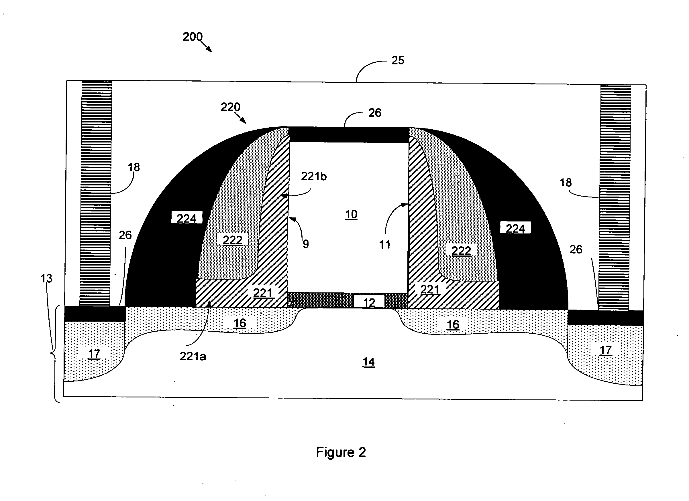
[0032] This disclosure presents embodiments of a field effect transistor structure and a method of forming the structure. As, stated above, the metal-oxide-semiconductor field-effect transistor (MOSFET) is the building bl...


PUM


Abstract

Disclosed is a MOSFET structure and method of fabricating the structure that incorporates a multi-layer sidewall spacer to suppress parasitic overlap capacitance between the gate conductor and the source/drain extensions without degrading drive current and, thereby, effecting overall MOSFET performance. In one embodiment, the multi-layer sidewall spacer is formed with a gap layer having a dielectric constant equal to one and a permeable low-K (e.g., less than 3.5) dielectric layer. In another embodiment, the multi-layer sidewall spacer is formed with a first L-shaped dielectric layer having a permittivity value of less than approximately three and a second dielectric layer. Either embodiment may also have a third nitride or oxide spacer layer. This third spacer layer provides increased structural integrity.

Description

BACKGROUND OF THE INVENTION [0001] 1. Field of the Invention [0002] The invention generally relates to a field effect transistor (FET) structure and, more particularly to a FET structure that incorporates a multi-layer low-K dielectric spacer to suppress capacitance coupling between the gate and the source and drain extensions. [0003] 2. Description of the Related Art [0004] The metal-oxide-semiconductor field-effect transistor (MOSFET) is the building block of very large scale integrated (VLSI) circuits in microprocessors and dynamic memories. MOSFETs are four-terminal devices with the terminals designated as the gate conductor, the source and drain regions and the channel. The channel and source and drain regions lie in a substrate on which the gate conductor is positioned. Generally, the channel lies directly beneath the gate conductor with the source and drain regions on either side of the channel. While most of the source and drain regions do not lie beneath the gate, small por...

Claims


Application Information

Patent Timeline
Patent Type & Authority Applications(United States)
IPC IPC(8): H01L29/78H01L21/469
CPCH01L29/4983H01L29/665H01L29/7833H01L29/6659H01L29/6656H01L29/4991
Inventor HUANG, ELBERT E.OLDIGES, PHILIP J.SHAHIDI, GHAVAM G.TYBERG, CHRISTY S.WANG, XINLINWISNIEFF, ROBERT L.
Owner GOOGLE LLC
Why Eureka
Try Eureka