Beam-induced etching

a beam-induced etching and beam-induced technology, applied in the field of localized beam-induced etching, can solve the problems of mask image defect, loss of transparency, and introduction of defects in the mask image that is transferred to the semiconductor substra

Active Publication Date: 2006-10-12
ECOLE POLYTECHNIQUE FEDERALE DE LAUSANNE (EPFL)
View PDF5 Cites 57 Cited by
  • Summary
  • Abstract
  • Description
  • Claims
  • Application Information

AI Technical Summary

Benefits of technology

[0019] In accordance with one aspect of the invention, a beam, such as an electron beam, is directed toward the material to be processed, along with a gas that etches the materi

Problems solved by technology

When the pattern is formed on the mask, typically by using computer controlled laser or electron beam systems to expose the desired mask pattern in a photoresist material, it is not unusual for the mask to have defects.
There are several problems with the use of gallium ion FIB systems to repair masks, particularly when used to repair opaque defects.
This loss of transparency, in turn, introduces defects in the mask image that is transferred to the semiconductor substrate.
The loss of transparency is particularly severe for the very short exposing light wavelengths used in modern photolithography processes, with the loss of transparency typically being between three and ten percent.
Second, the sputtering process of the focused ion beam is relatively unselective.
While an opaque defect is being removed by the ion beam, substrate material at the edge of the defect is also attacked, and the result is a trench of damaged substrate material around the defect.
Third, the sputtering of material by the ion beam leads to ejection of material in all directions, and some of this ejected material comes to rest on adjacent surfaces.
This effect, known as redeposition, limits t

Method used


Image

  • Beam-induced etching
  • Beam-induced etching
  • Beam-induced etching

Examples


Embodiment Construction

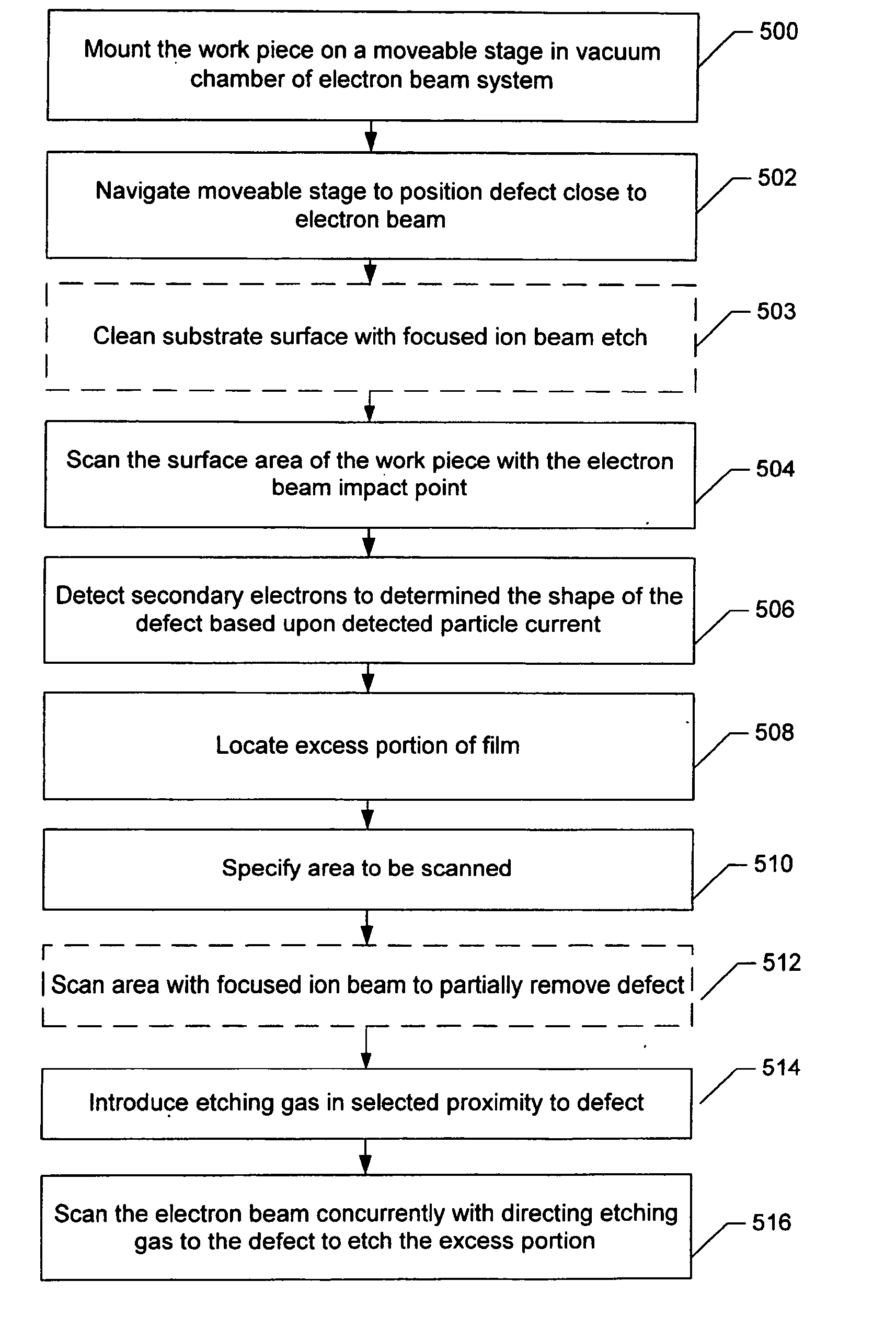
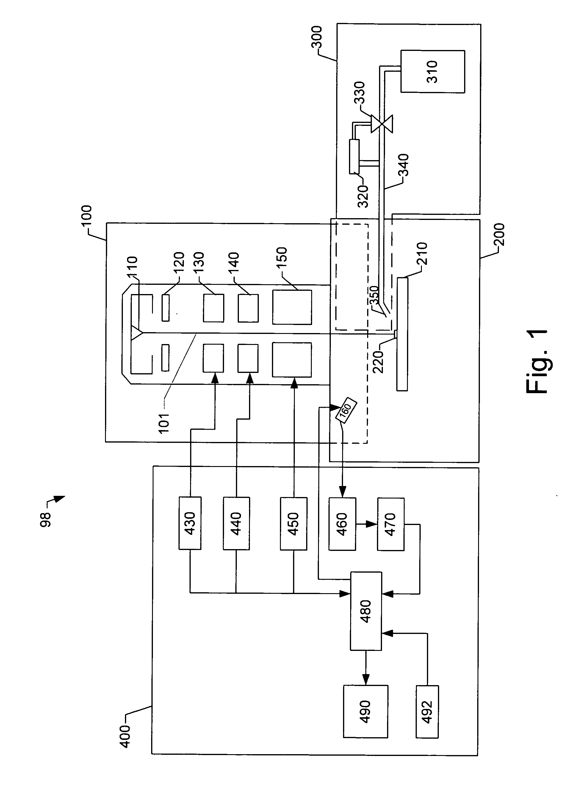
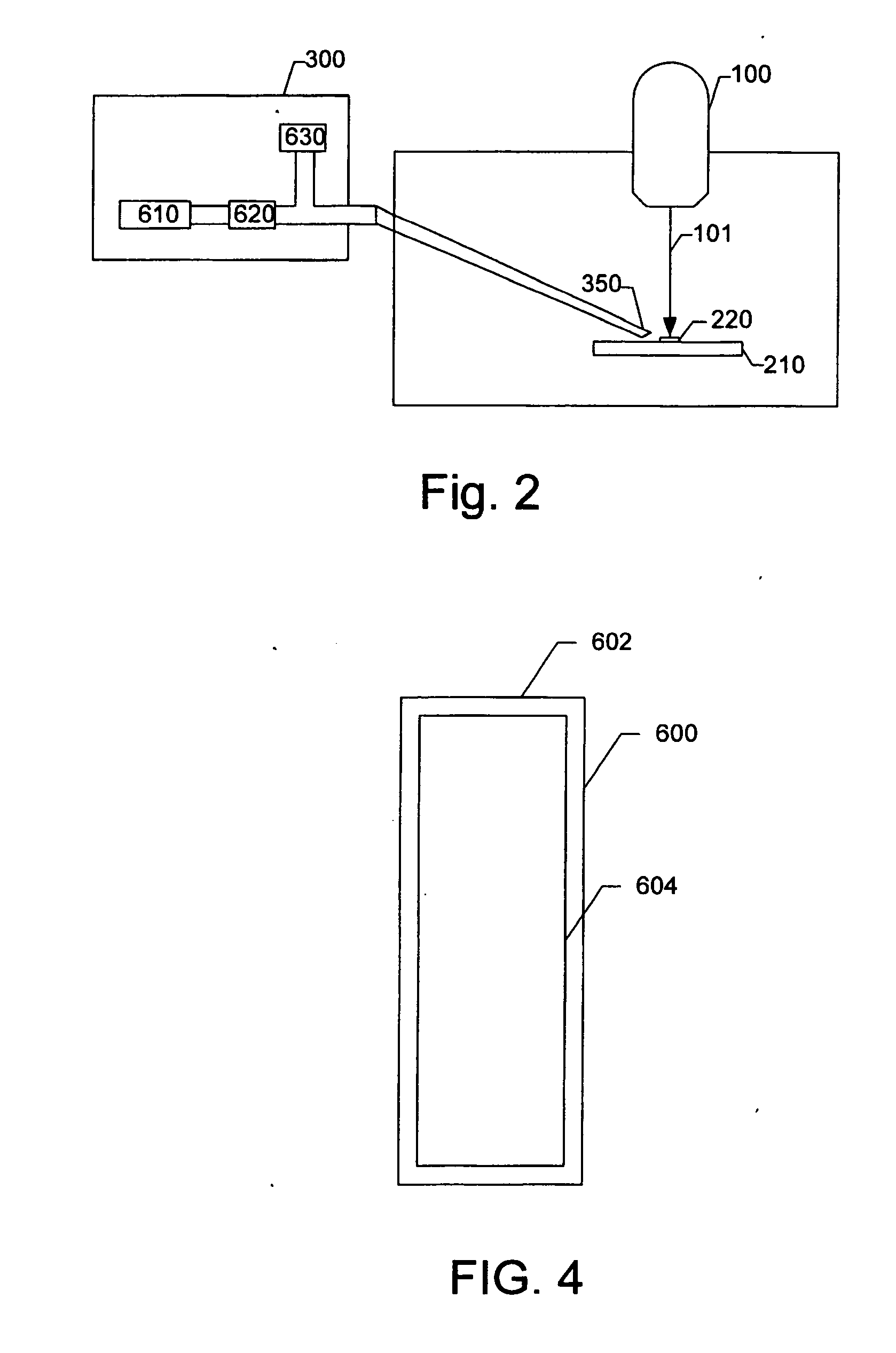
[0026] The present invention provides methods for locally removing material using a beam. The invention provides etchants that are useful for selectively etching certain materials in the presence of an activating beam, such as a charged particle beam or a laser beam. Some embodiments are particularly useful for etching chromium materials and can be used for electron beam-induced etching.

[0027]“Chromium material” as used herein includes any material containing chromium, such as the metallic chromium, partially oxidized chromium and partially nitrided chromium. Such chromium materials are commonly used as absorbing layers in photolithography masks. The invention is therefore particularly useful for photolithography mask repair. The invention can be used as part of a serial process, in which a single beam performs operations one after another, or in a parallel process, in which multiple beams operate simultaneously on one or more work pieces, either on the same or on different areas o...


PUM

PropertyMeasurementUnit
Timeaaaaaaaaaa
Adsorption energyaaaaaaaaaa
Electric dipole momentaaaaaaaaaa

Abstract

A method and apparatus for local beam processing using a beam activated gas to etch material are described. Compounds are disclosed that are suitable for beam-induced etching. The invention is particularly suitable for electron beam induced etching of chromium materials on lithography masks. In one embodiment, a polar compound, such as ClNO2 gas, is activated by the electron beam to selectively etch a chromium material on a quartz substrate. By using an electron beam in place of an ion beam, many problems associated with ion beam mask repair, such as staining and riverbedding, are eliminated. Endpoint detection is not critical because the electron beam and gas will not etch significantly the substrate.

Description

TECHNICAL FIELD OF THE INVENTION [0001] The present invention relates to the field of localized beam-induced etching and, in particular, to a method and apparatus for using a beam to create or alter microscopic structures. BACKGROUND [0002] Photolithography processes are widely used in the fabrication of integrated circuits. In a typical photolithography process, a thin layer of a photoactive material called “photoresist” is deposited onto the surface of a semiconductor substrate, such as a silicon wafer. The photoresist can be composed of any of a number of different materials whose chemical structure changes when exposed to a certain type of radiation. This change in chemical structure can cause the photoresist to become more soluble, in the case of a positive photoresist, or less soluble, in the case of a negative photoresist, in a chemical solution referred to as a developer. [0003] A photolithography mask in the shape of a desired circuit pattern is used as a template to transf...

Claims


Application Information

Patent Timeline
IPC IPC(8): H01J37/08G21G5/00A61N5/00G21K5/10G03F1/00
CPCC23F4/00C23F4/02H01J2237/31744G03F1/74G03F1/72
Inventor BRET, TRISTANHOFFMANN, PATRIKROSSI, MICHELMULTONE, XAVIER
Owner ECOLE POLYTECHNIQUE FEDERALE DE LAUSANNE (EPFL)
Why Eureka
Try Eureka