Semiconductor device using solid phase epitaxy and method for fabricating the same

a semiconductor device and solid phase epitaxy technology, applied in the field of semiconductor device contact plugs, can solve the problems of device degradation phenomena, internal pressure degradation, data retention time degradation of semiconductor devices, etc., and achieve the effect of high resistivity

Inactive Publication Date: 2006-10-26
SK HYNIX INC
View PDF13 Cites 19 Cited by
  • Summary
  • Abstract
  • Description
  • Claims
  • Application Information

AI Technical Summary

Benefits of technology

[0027] The present invention relates to a semiconductor device using an epitaxial silicon layer as a contact plug and a method for fabricating the same, wherein the semiconductor device is capable of forming the epitaxial silicon layer as

Problems solved by technology

Accordingly, device degradation phenomena such as degradation in a data retention time of the semiconductor device have been generated.
However, the above described method to increase the phosphorus concentration results in degradation of an internal pressure due to a significant out-diffusion of the dopants and the decrease of a data retention time of a device.
It may be very difficult to use the polysilicon at a contact process of a semiconductor device with a size equal to or less than approximately sub-100 nm requiring a very low contact resistance.
However, the SEG process uses a high temperature process performed at a temperature of approximately 850° C. and thus, the SEG process cannot be applied to a current process for fabricating a semiconductor device.
Thus, the increased doping concentration of P

Method used


Image

  • Semiconductor device using solid phase epitaxy and method for fabricating the same
  • Semiconductor device using solid phase epitaxy and method for fabricating the same
  • Semiconductor device using solid phase epitaxy and method for fabricating the same

Examples


Embodiment Construction

[0036] Hereinafter, detailed descriptions on embodiments of the present invention will be provided with reference to the accompanying drawings.

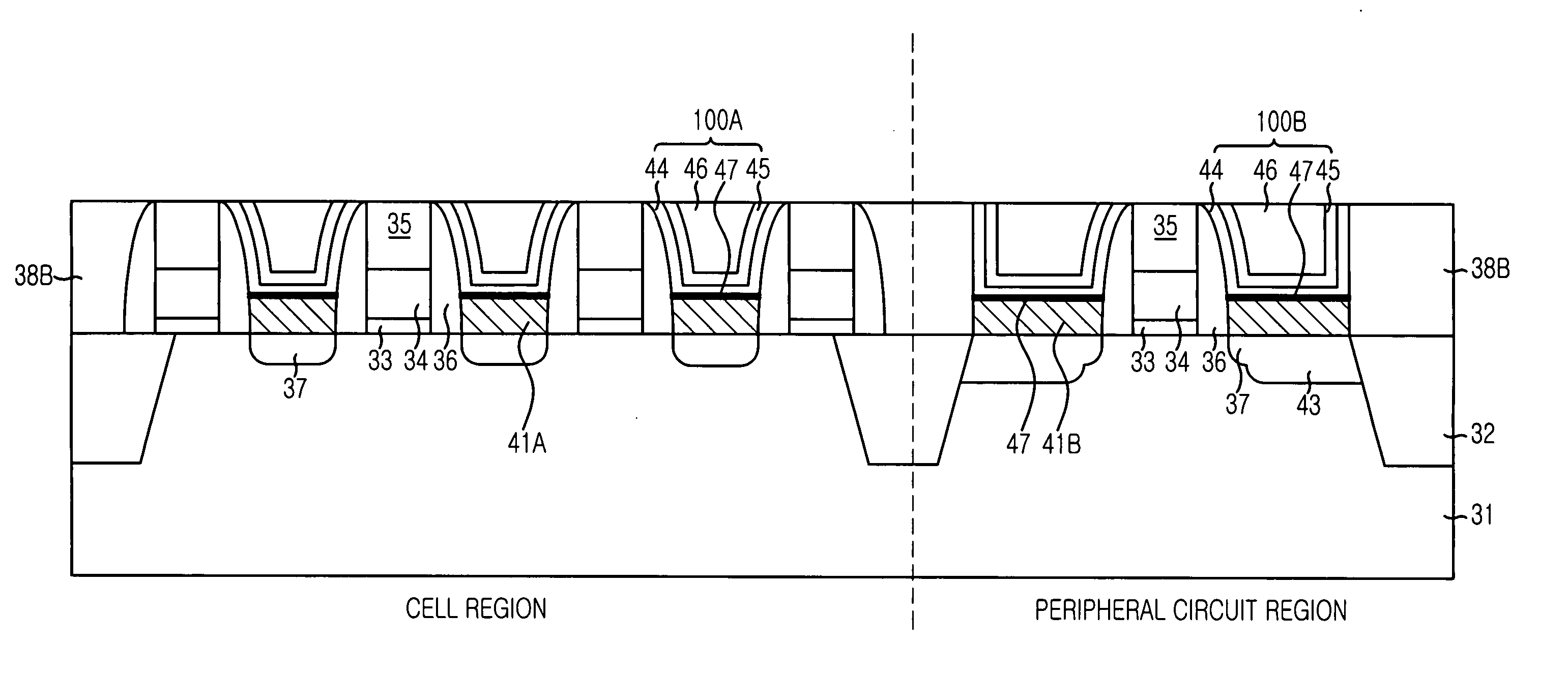
[0037]FIG. 3 is a cross-sectional view illustrating a semiconductor device structure in accordance with the present invention.

[0038] As shown in FIG. 3, the semiconductor device structure includes a substrate 31 defined with a cell region and a peripheral circuit region, a self-aligned contact (SAC) formed by sequentially stacking a first contact layer 41A that is an epitaxial layer, a second contact layer 100A that is a metal material on the cell region of the substrate 31, an elevated source / drain (ESD) formed by sequentially stacking a first ESD layer 41B that is an epitaxial layer, and a second ESD layer 100B that is a metal material on the peripheral circuit region of the substrate 31.

[0039] Referring to FIG. 3, in accordance with one embodiment of the present invention, the first contact layer 41A forming the SAC and the epitaxial la...


PUM


Abstract

A semiconductor device includes an epitaxial layer using a solid phase epitaxy (SPE) process; a first metal layer on the epitaxial layer; a nitride-based barrier metal layer on the first metal layer; a second metal layer on the barrier metal layer; and a metal silicide layer formed between the epitaxial layer and the first metal layer after a post-annealing process.

Description

FIELD OF THE INVENTION [0001] The present invention relates to a method for fabricating a semiconductor device; and more particularly, to a contact plug of a semiconductor device and a method for fabricating the same. DESCRIPTION OF RELATED ARTS [0002] As the scale of integration has been increasing, while the size of a semiconductor device has been decreasing, dynamic random access memory (DRAM) devices have been influenced by a gradual reduction of contact size within a cell transistor. As size reduction and high integration of semiconductor devices have occurred, there has also been an increase in a contact resistance and a decrease in an operation current due to a decrease in a contact area resulting from a decrease in the contact size. Accordingly, device degradation phenomena such as degradation in a data retention time of the semiconductor device have been generated. [0003] In order to reduce the contact resistance and improve the operation current, a method to increase a dop...

Claims


Application Information

Patent Timeline
IPC IPC(8): H01L29/76
CPCH01L21/02063H01L2924/0002H01L21/28562H01L21/31053H01L21/76819H01L21/76846H01L21/76867H01L21/76889H01L21/76897H01L27/10855H01L27/10885H01L27/10894H01L21/28525H01L2924/00H10B12/0335H10B12/09H10B12/482A47J27/002A47J36/00Y10S220/912
Inventor AHN, TAE-HANG
Owner SK HYNIX INC
Why Eureka
Try Eureka