

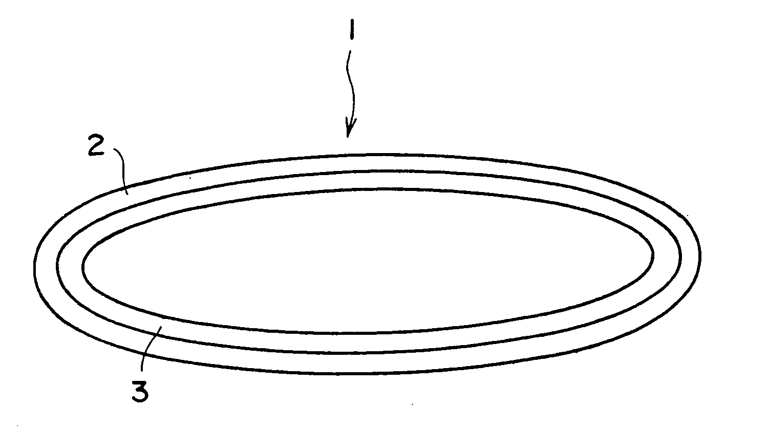
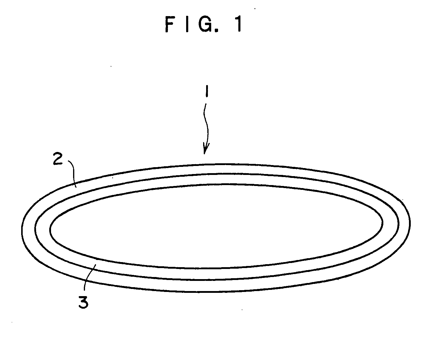
Semiconductive belt and image forming apparatus using the semiconductive belt
a semi-conductive belt and image forming technology, applied in the direction of electrographic process apparatus, instruments, optics, etc., can solve the problems of color deviation, extremely inferior toner transfer property of elastic belts with reinforcing materials, and poor durability of elastic belts, so as to reduce the deformation of surface layers, and reduce the deformation of elastic belts
- Summary
- Abstract
- Description
- Claims
- Application Information
AI Technical Summary
Benefits of technology
Problems solved by technology
Method used
Image

Examples
example 1
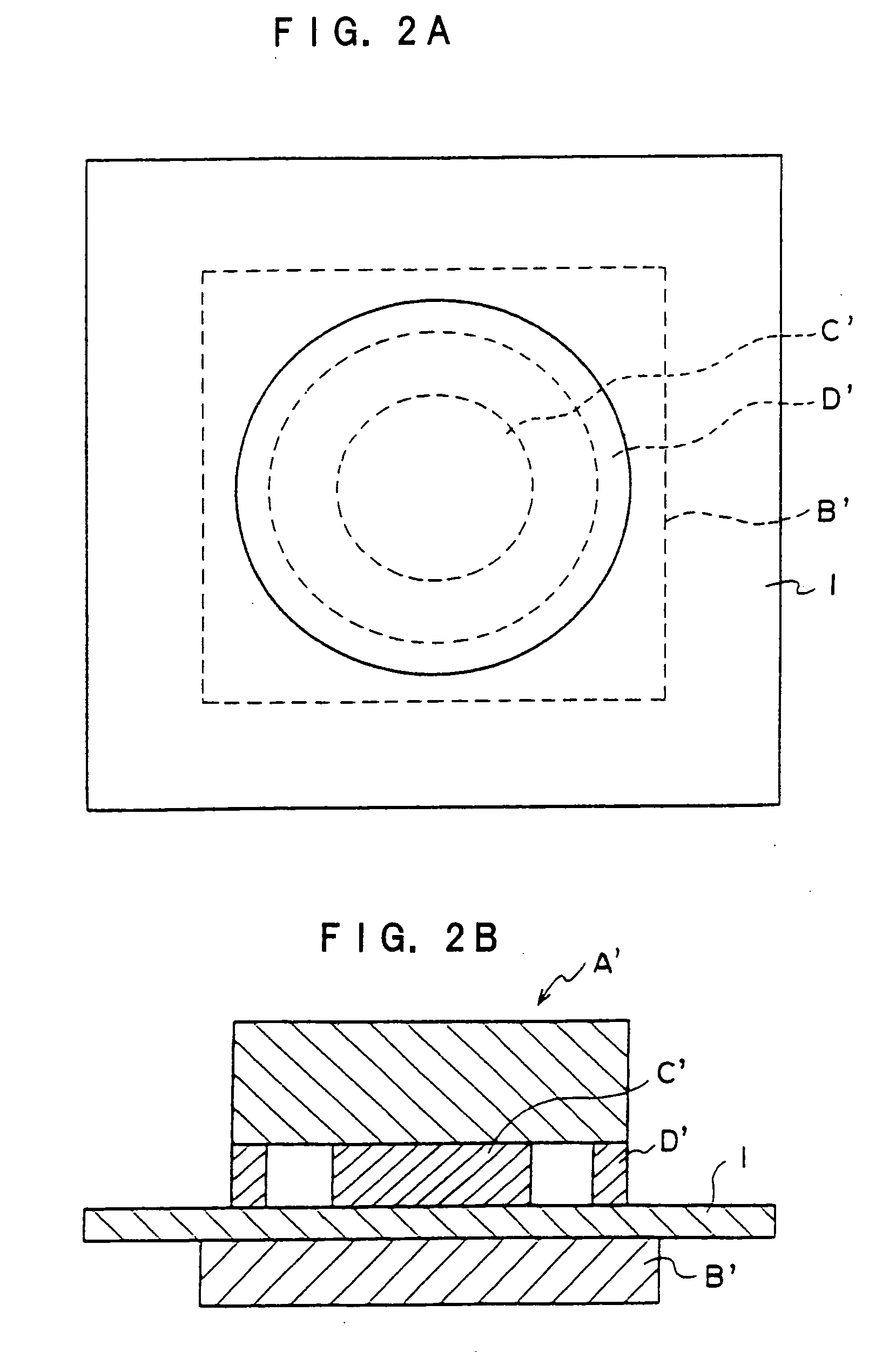
[0120] A cylindrical metal mold with an outer diameter of 168 mm and length of 500 mm is coated with the substrate (A), and a solution of the surface layer material (A) is uniformly applied on the outside surface thereof. While rotating in a heating furnace, the metal mold is heated for 120 minutes at a temperature of 80° C. to cure the surface layer material (A). After the heating process, inside of the furnace is returned to normal temperature and pressure, and the metal mold is taken out. The resin is removed from the metal mold, and a semiconductive belt with an inner diameter of 168 mm, width of 350 mm, and thickness of 0.33 mm is obtained. With respect to the thickness of each layer of this belt, the surface layer has a 0.25 mm thickness, and the substrate has a 0.08 mm thickness. Volume resistivity of the surface layer is 7×10¹¹ ohm-cm. Durometer hardness of the surface layer is A45 / S.
[0121]—Durometer Hardness—
[0122] Durometer hardness of the surface layer conforms to JIS K ...
example 2
[0123] A semiconductive belt with an inner diameter of 168 mm, width of 350 mm, and thickness of 0.33 mm is prepared in the same manner as in example 1 except that the surface layer material (B) is used instead of the surface layer material (A). With respect to the thickness of each layer of this belt, the surface layer has a 0.25 mm thickness, and the substrate has a 0.08 mm thickness. Volume resistivity of the surface layer is 9×10¹¹ ohm-cm. Durometer hardness of the surface layer is A32 / S.
example 3
[0124] A semiconductive belt with an inner diameter of 168 mm, width of 350 mm, and thickness of 0.48 mm is prepared in the same manner as in example 1 except that the substrate (B) is used instead of the substrate (A), and that the surface layer material (C) is used instead of the surface layer material (A). With respect to the thickness of each layer of this belt, the surface layer has a 0.40 mm thickness, and the substrate has a 0.08 mm thickness. Volume resistivity of the surface layer is 1×10¹³ ohm-cm. Durometer hardness of the surface layer is A55 / S.
PUM
 Abstract
Description
Claims
Application Information