
Inspection method and inspection system using charged particle beam

Active Publication Date: 2006-11-02
HITACHI HIGH-TECH CORP
View PDF11 Cites 20 Cited by
  • Summary
  • Abstract
  • Description
  • Claims
  • Application Information

AI Technical Summary

Benefits of technology

[0023] A first object of the present invention is to prevent degradation in shadow contrast due to inclination of the center axis of secondary electrons and to perform constantly stable detection of shallow unevenness even when the secondary electrons are accelerated to high speeds by an electromagnetic field efficient to obtain high resolution. A second object of the invention is to prevent degradation in elevation angle separation accuracy attributable to a shift between the center axis of a separation detector and the center axis of secondary electrons in course of detection of secondary electrons in which secondary electrons are separated in accordance with elevation angles in the outgoing or emitting direction. Further, a third object of the invention is to reduce the non-uniformity in the field of view and loss of secondary electron signal attributable to fine convergence of secondary electrons.
[0025] According to the present invention, in inspection of a partially completed substrate of a semiconductor device having circuit patterns, shallow unevenness and minute foreign matters can be detected with high sensitivity while maintaining high resolution and can be reviewed and classified. Thus, semiconductor products can be monitored with high sensitivity to make it easy to specify or identify causes of defects.

Problems solved by technology

The acceleration of secondary electrons to high speeds as described above, however, gives rise to a new problem.
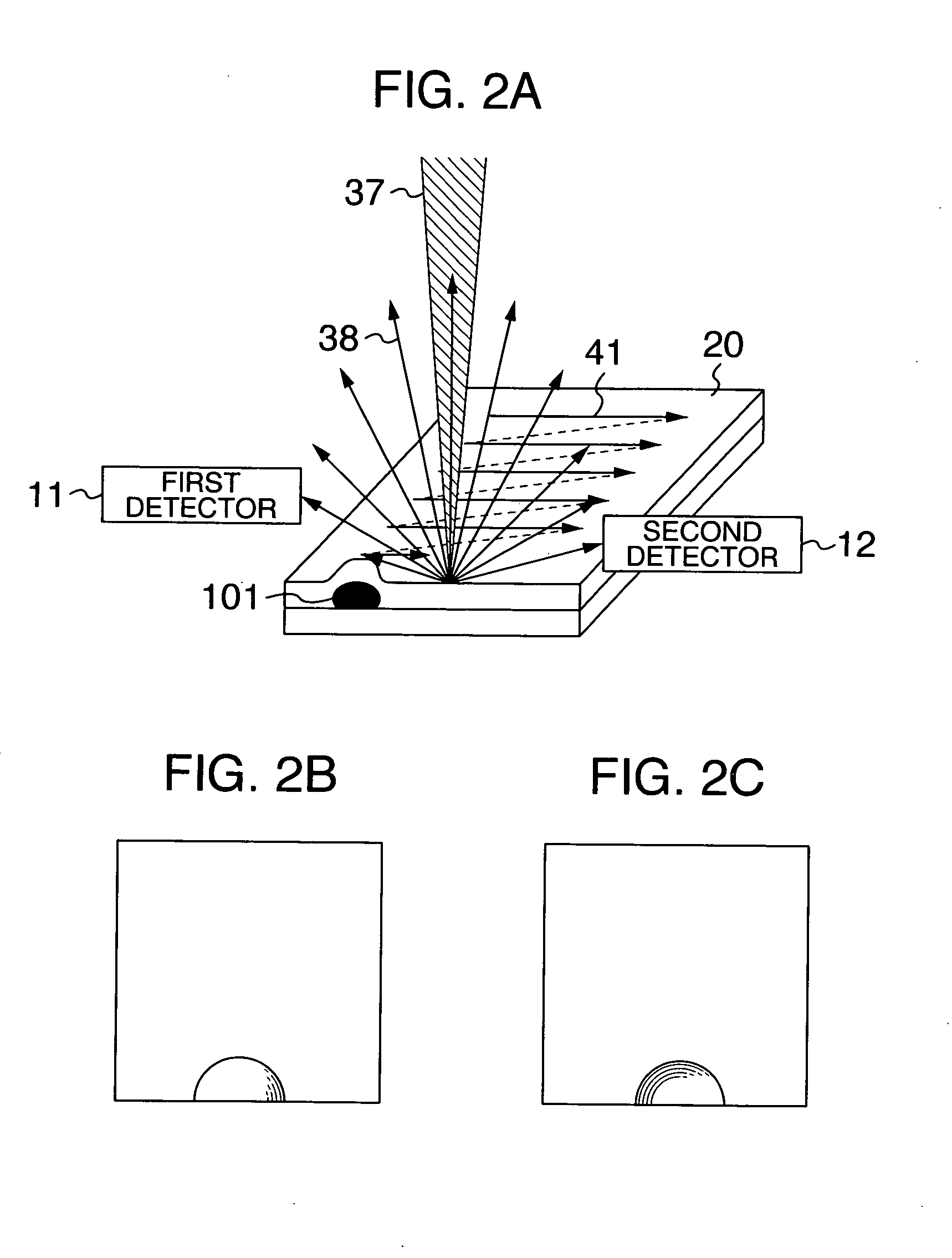
As compared to secondary electrons not speeded up, highly accelerated secondary electrons are converged relatively finely upon arrival at the detection surface, with the result that, if the center trajectory of secondary electrons is slightly inclined, the balance between right and left angle distributions is disturbed at the time of detection of the secondary electrons by the detectors and a problem of a failure to keep uniform separation arises.
But in the case of, for example, the review SEM in which acceleration of secondary electrons to high speeds, highly contrasted shadow images and highly raised throughput are necessary, the inclination of the optical axis of secondary electrons greatly affects the signal acquisition and eventually the decision of defects.
This inconvenience leads to the possibility that in trying to obtain contrast of a very shallow uneven portion, a shadow contrast is so buried in another signal as to disappear.
In addition, the apparatus operating as semiconductor reviewer cannot obtain a shadow contrast correctly reflecting a topographic shape, suffering from the possibility that erroneous recognition of defect shapes results.
Further, when only a component of low elevation of secondary electrons is detected as a component reflecting a shadow contrast, separate detection of secondary electrons in the elevation angle direction is needed and in such a case, if the center axis of the secondary electrons shifts from the center axis of the detector, there arises a problem that the elevation angles cannot be separated uniformly irrespective of azimuth angles.
And also, the inclination of the optical axis of secondary electrons depends on an adjusted condition of the apparatus and even when the same topographic sample is watched, different contrasts are disadvantageously obtained in accordance with the adjusted condition of the apparatus.

Method used


Image

  • Inspection method and inspection system using charged particle beam
  • Inspection method and inspection system using charged particle beam
  • Inspection method and inspection system using charged particle beam

Examples


embodiment 1

[0050] In the present embodiment, an instance will be described in which defect classifying is done by using a review SEM.

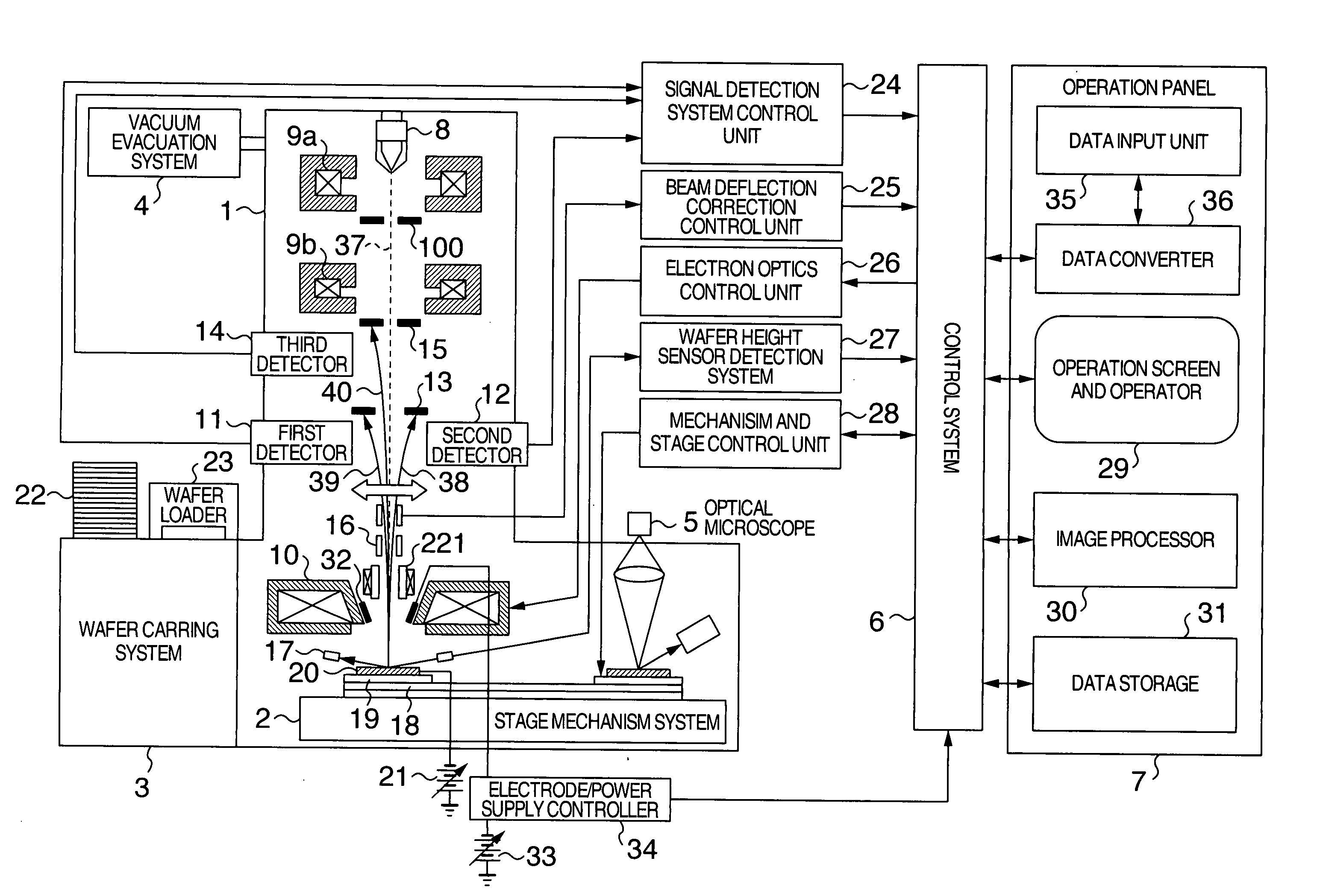
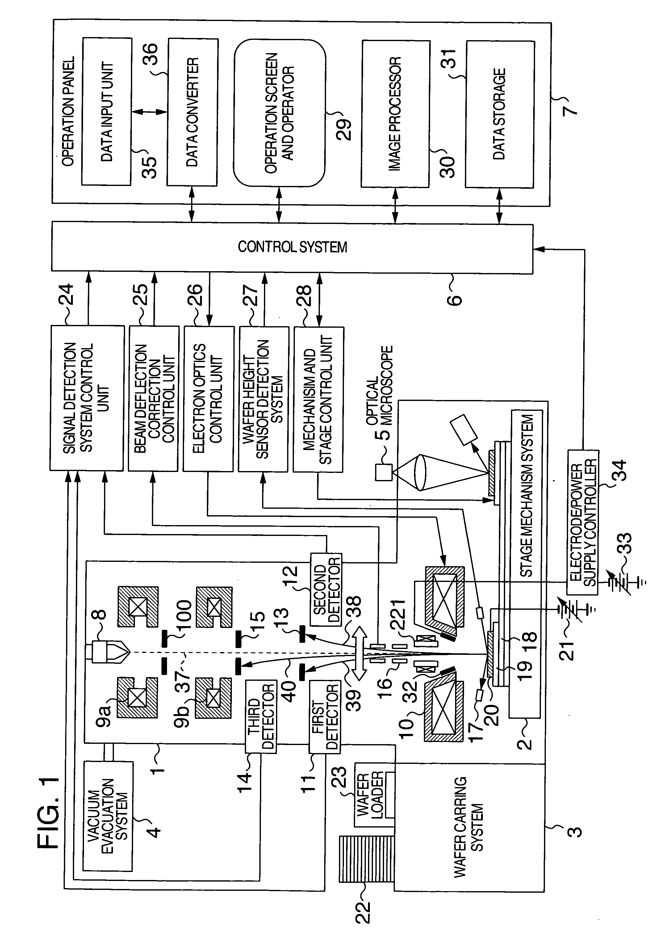
[0051] The review SEM is constructed as exemplified in FIG. 1. The present apparatus comprises an electron optics 1, a stage mechanism system 2, a wafer carrying system 3, a vacuum evacuation system 4, an optical microscope 5, a control system 6 and an operation panel 7.

[0052] The electron optics 1 includes an electron source 8, a condenser lens 9, an aperture 100, an objective lens 10, a first detector 11, a second detector 12, a first reflecting plate 13, a third detector 14, a second reflecting plate 15, a scan deflector 16, a wafer height sensor 17, an accelerating electrode 32 arranged to oppose the stage, an electrode power supply 33, an electrode power supply controller 34 and a deflector for secondary electrons (E×B deflector) 221. The construction and operation of the principal part of electron optics have already been explained with reference to FIG. ...

embodiment 2

[0078] Next, a second embodiment will be described. The overall construction is similar to that of the first embodiment shown in FIGS. 1 and 4. Structurally, in the second embodiment, an E×B deflector 221 is constructed of a quaternary electrode and a quaternary magnetic pole in order that secondary electrons can be deflected at all azimuth angles. Accordingly, alignment of secondary electrons can be accomplished in not only the separation direction of reflecting plate 13 (x direction in the figure) but also a direction vertical to the sheet of drawing (y direction). Through this, the center axis direction of secondary electrons can be corrected for shift in y direction in relation to the aperture formed in the reflecting plate 13. In addition, secondary electrons can be so adjusted as to impinge upon the reflecting plate 15 at a desired part. As will be seen from the above, with the optical axis of secondary electrons aligned in both the x and y directions, signals can be obtained ...

embodiment 3

[0079] Next, a third embodiment will be described. Structurally, the present embodiment is identical to the second embodiment with the only exception that reflecting plates 13 and 15 are constructed as shown in FIG. 9 when viewed from the specimen. More particularly, where the direction of secondary electron separation by the reflecting plate 13 is in x direction, a direction vertical to the x direction is y direction and the optical axis of the primary electron beam is in z direction, a beam pass aperture 213 in the reflecting plate 13 has an ellipsoidal shape having a major axis in y direction and a minor axis in x direction and a beam pass aperture 215 in the reflecting plate 15 has a circular shape having a diameter smaller than the major axis of the aperture 213. Needless to say, a pass aperture 213 having a rectangular shape or the like can attain the same effect and can be included in the present invention. For operation, this structure is used in combination with the quatern...


PUM


Abstract

In an electric immersion lens having high resolution capability, secondary electrons generated from a specimen are accelerated to suppress the dependency of rotational action of the secondary electrons applied thereto by an objective lens upon energy levels of the secondary electrons and when selectively detecting low and high angle components of elevation and azimuth as viewed from a secondary electron generation site by means of an annular detector interposed between an electron source and the objective lens, the secondary electrons are adjusted and deflected by means of an E×B deflector such that the center axis of secondary electrons converged finely under acceleration is made to be coincident with the center axis of a low elevation signal detection system and the secondary electrons are deviated from an aperture of a high elevation signal detection system.

Description

BACKGROUND OF THE INVENTION [0001] The present invention relates to a charged particle beam detection system of charged particle beam apparatus and a charged particle beam apparatus equipped with the charged particle beam detection system and more particularly, to a scanning electron microscope (SEM) for forming an image of a signal of electrons such as secondary electrons generated from a specimen while scanning an electron beam. More specifically, the present invention is concerned with method and system for inspecting a substrate having minute circuit patterns such as a semiconductor device or liquid crystal device and particularly, concerned with a review SEM technology of performing pattern inspection and defect review of the semiconductor device and a photo-mask as well. [0002] As generally known, in the SEM for scanning an electron beam on a specimen to form an image of a signal of electrons such as secondary electrons generated from the specimen, the contrast of an acquired ...

Claims


Application Information

Patent Timeline
IPC IPC(8): G01N23/00
CPCG01N23/2251H01J37/147H01J37/244H01J2237/24507H01J2237/1501H01J2237/1508H01J2237/2449H01J37/28
Inventor FUKADA, ATSUKOSATO, MITSUGUSUZUKI, NAOMASANISHIYAMA, HIDETOSHIFUKUDA, MUNEYUKITAKAHASHI, NORITSUGU
Owner HITACHI HIGH-TECH CORP
Learn More