Split-channel antifuse array architecture

a technology of anti-fuse arrays and transistors, which is applied in the direction of digital storage, semiconductor/solid-state device details, instruments, etc., can solve the problems of many limits on the array size, few kilo ohms leakage between the source and the drain, and the possibility of anti-fuse self-healing under current stress, etc., to achieve simple and reliable, reduce the over-voltage exposure of switching elements, and reduce the effect of over-vol

Inactive Publication Date: 2006-11-02
SYNOPSYS INC
View PDF50 Cites 147 Cited by
  • Summary
  • Abstract
  • Description
  • Claims
  • Application Information

AI Technical Summary

Benefits of technology

[0025] It is, therefore, desirable to provide a simple and reliable, high density, anti-fuse array architecture suitable for implementation in standard CMOS technology, without any additional processing steps and with limited over-voltage exposure of switching elements. It is also desirable to provide a testing method for the anti-fuse arrays to be effectively tested prior to shipment and permanent programming in the

Problems solved by technology

The possibility of anti-fuse self-healing under current stress appeared to be the main roadblock for application of this technology in such areas like PROMs, PLDs and FPGAs, where constant fuse stress was required.
They discovered that with 0.5 um technology, the BVDSS for the nmos transistor is not only in the order of 6.5V, but once the S-D punch through occurs it creates permanent damage resulting in few kilo ohms leakage between the source and the drain.
This puts many limits on the array size, affects driver size and impacts reliability and effectiveness of programming.
This leads to large N++ junction leakage current, and again limits array size.
This is not

Method used


Image

  • Split-channel antifuse array architecture
  • Split-channel antifuse array architecture
  • Split-channel antifuse array architecture

Examples


Embodiment Construction

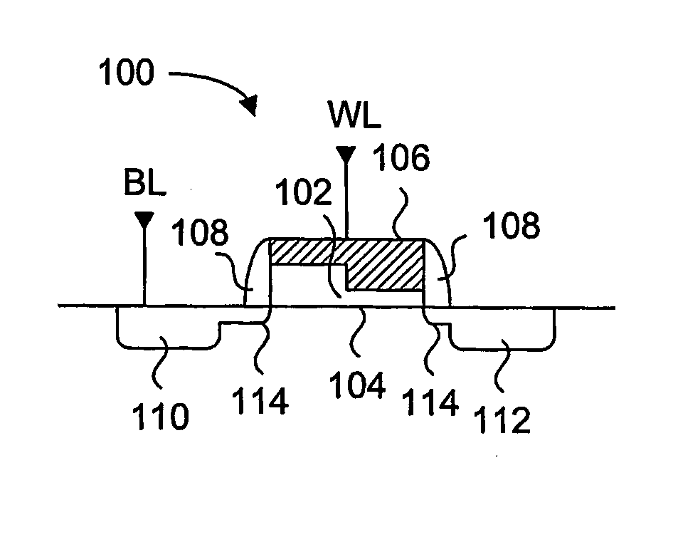
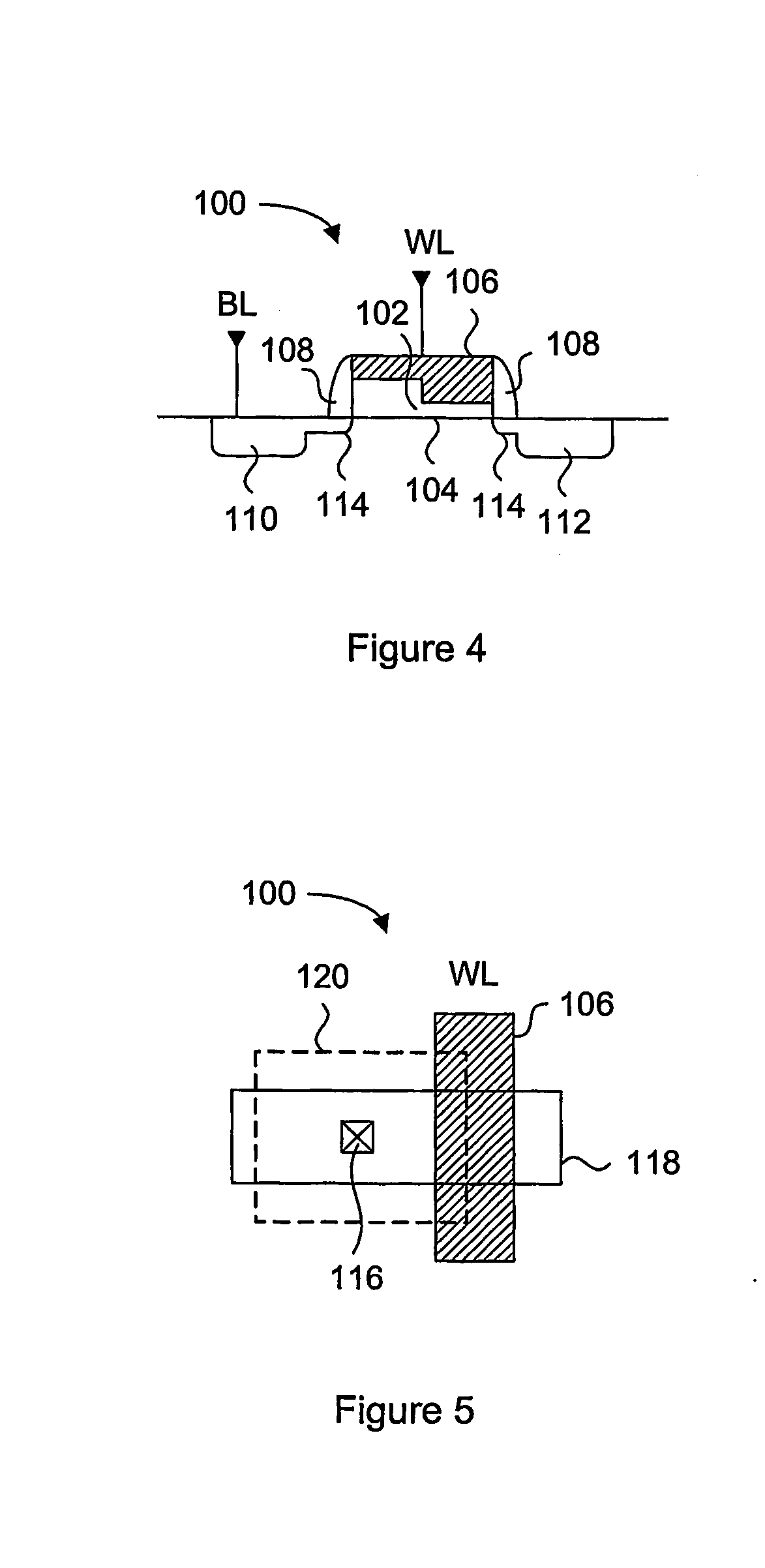
[0058] Generally, the present invention provides a variable thickness gate oxide anti-fuse transistor device that can be employed in a non-volatile, one-time-programmable (OTP) memory array application. The anti-fuse transistor can be fabricated with standard CMOS technology, and is configured as a standard transistor element having a source diffusion, gate oxide, polysilicon gate and optional drain diffusion. The variable gate oxide underneath the polysilicon gate consists of a thick gate oxide region and a thin gate oxide region, where the thin gate oxide region acts as a localized breakdown voltage zone. A conductive channel between the polysilicon gate and the channel region can be formed in the localized breakdown voltage zone during a programming operation. In a memory array application, a wordline read current applied to the polysilicon gate can be sensed through a bitline connected to the source diffusion, via the channel of the anti-fuse transistor. More specifically, the p...


PUM


Abstract

Generally, the present invention provides a variable thickness gate oxide anti-fuse transistor device that can be employed in a non-volatile, one-time-programmable (OTP) memory array application. The anti-fuse transistor can be fabricated with standard CMOS technology, and is configured as a standard transistor element having a source diffusion, gate oxide, polysilicon gate and optional drain diffusion. The variable gate oxide underneath the polysilicon gate consists of a thick gate oxide region and a thin gate oxide region, where the thin gate oxide region acts as a localized breakdown voltage zone. A conductive channel between the polysilicon gate and the channel region can be formed in the localized breakdown voltage zone during a programming operation. In a memory array application, a wordline read current applied to the polysilicon gate can be sensed through a bitline connected to the source diffusion, via the channel of the anti-fuse transistor. More specifically, the present invention provides an effective method for utilizing split channel MOS structures as an anti-fuse cell suitable for OTP memories.

Description

CROSS REFERENCE TO RELATED APPLICATIONS [0001] This application claims the benefit of priority of U.S. Provisional Patent Application No. 60 / 568,315 filed May 6, 2004, which is incorporated herein by reference.FIELD OF THE INVENTION [0002] The present invention relates generally to non-volatile memory cells. In particular, the present invention relates to split-channel anti-fuse transistors. BACKGROUND OF THE INVENTION [0003] Over the past 30 years, anti-fuse technology has attracted significant attention of many inventors, IC designers and manufacturers. An anti-fuse is a structure alterable to a conductive state, or in other words, an electronic device that changes state from not conducting to conducting. Equivalently, the binary states can be either one of high resistance and low resistance in response to electric stress, such as a programming voltage or current. There have been many attempts to develop and apply anti-fuses in microelectronic industry, but the most successful ant...

Claims


Application Information

Patent Timeline
IPC IPC(8): H01L29/00G11C11/40G11C11/401G11C17/16H01L21/28H01L21/331H01L21/336H01L23/525H01L27/10H01L27/115H01L29/423H01L29/66H01L29/78
CPCG11C17/16G11C17/18H01L2924/0002H01L21/28211H01L23/5252H01L27/10H01L27/101H01L27/112H01L27/11206H01L29/42368H01L29/4238H01L29/42384H01L29/7833H01L2924/00H10B20/00H10B20/20H01L29/66
Inventor KURJANOWICZ, WLODEK
Owner SYNOPSYS INC
Why Eureka
Try Eureka