
Method for electrochemical etching of semiconductor material using positive potential dissolution (PPD) in HF-free solutions

a technology of positive potential dissolution and electrochemical etching, which is applied in the direction of electrical machining apparatus, cells, electrical equipment, etc., can solve the problems of undesirable use of media containing hf and inability to use positive (anodic) biasing

Inactive Publication Date: 2006-11-16
TECHNION RES & DEV FOUND LTD
View PDF3 Cites 15 Cited by
  • Summary
  • Abstract
  • Description
  • Claims
  • Application Information

AI Technical Summary

Benefits of technology

[0008] It is a further object of the present invention to provide a method for etching (polishing / texturing) a semiconductor material, comprising simple and inexpensive steps.
[0009] It is a further object of the present invention to provide a method for fast etching (polishing / texturing) a semiconductor material, using non-toxic chemicals.
[0010] The method of the present invention provides a technique of positive potential dissolution (PPD), based on applying positive (anodic) potentials higher than +10 volts relative to a standard reference electrode, such as a standard calomel electrode (SCE). In particular, application is made of a range of potentials between about plus 10 volt and plus 750 volts relative to a standard reference electrode, such as a SCE, during conditions of wet etching. Application of the potential may be combined with illumination of the positively biased exposed silicon surface, allowing silicon etching. The rate of silicon etching (texturing / polishing) in alkaline media, for example, KOH solutions, could be significantly increased by using high positive (anodic) biasing, above passive potentials of the silicon that is exposed to (contacted and wetted by) the alkaline etching solution, with or without illumination of the positively biased exposed silicon surface.
[0017] In a preferred embodiment of the present invention, the positive potential dissolution (PPD) texturing method features subjecting a polished material, or an as-cut, semiconductor material to an etching solution. The method also includes positive biasing at atypically highly positive (anodic) potentials, more positive than plus 10 volts relative to a standard reference electrode. Specifically controlling and directing illumination by light, preferably, processed non-ambient light, incident upon the positively biased polished / as-cut semiconductor material surface contacted and wetted by the HF-free etching solution. The specifically controlled and directed illumination of the positively biased semiconductor material surface contacted and wetted by the etching solution significantly increases the value of the anodic current density (A / cm2) of the semiconductor material.
[0018] Accordingly, in this preferred embodiment, the positive biasing at atypically highly positive (anodic) potentials, preferably but not essentially, combined with specifically controlling and directed illumination by light of the semiconductor material surface contacted and wetted by the etching solution, for a period of time, corresponds to a positive synergistic effect on the rate and extent of etching of the semiconductor material, and therefore, on the type of etched semiconductor material formed therefrom.

Problems solved by technology

However, the use of media containing HF is undesirable because it is accompanied by serious environmental issues relating to its handling and disposal.
Thus, except when etching / texturing silicon in HF solutions, positive (anodic) biasing has not been in use.

Method used


Image

  • Method for electrochemical etching of semiconductor material using positive potential dissolution (PPD) in HF-free solutions
  • Method for electrochemical etching of semiconductor material using positive potential dissolution (PPD) in HF-free solutions
  • Method for electrochemical etching of semiconductor material using positive potential dissolution (PPD) in HF-free solutions

Examples


Embodiment Construction

[0028] The principles and operation of a method and an apparatus according to the present invention may be better understood with reference to the drawings and the accompanying description, it being understood that these drawings are given for illustrative purposes only and are not meant to be limiting.

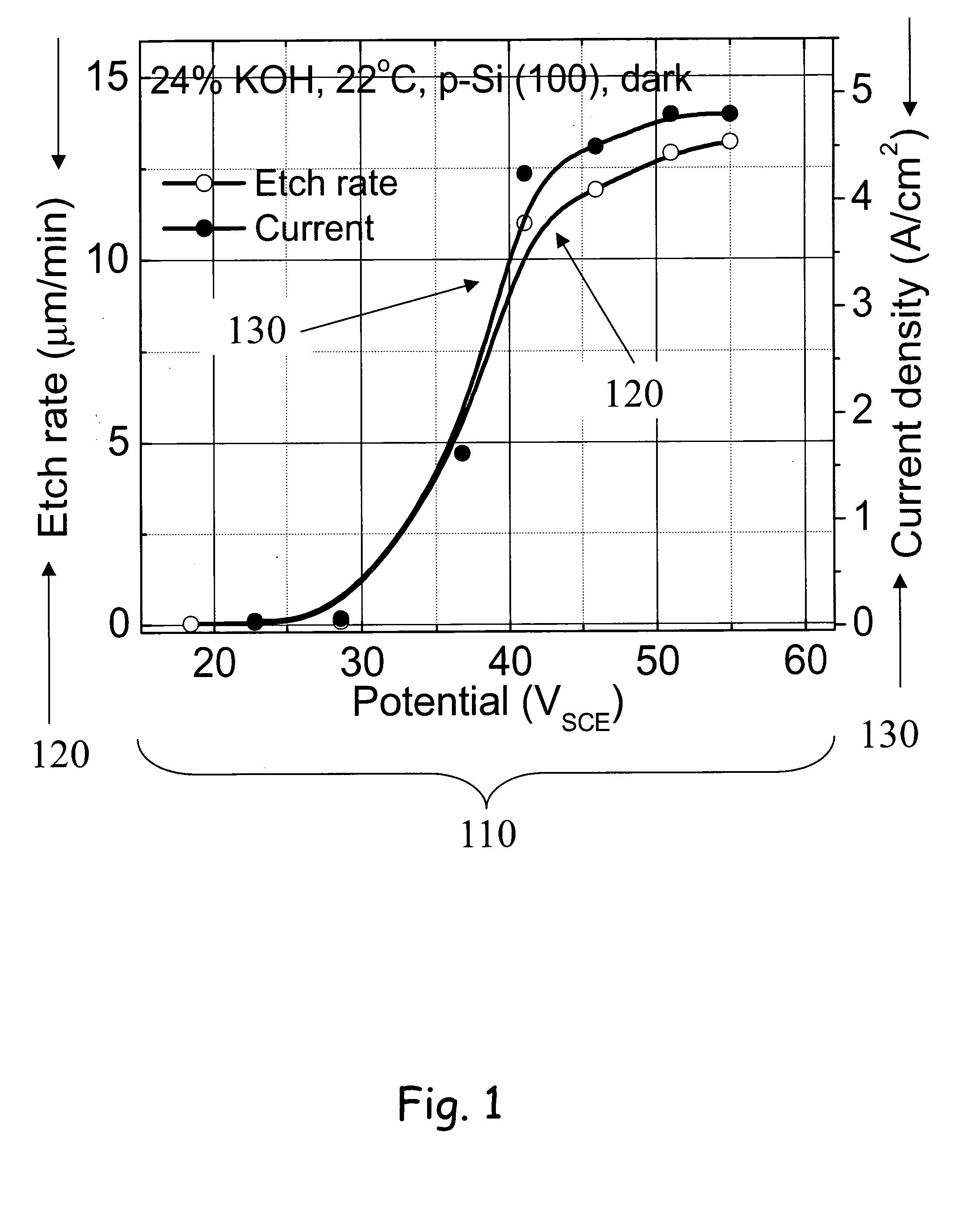
[0029]FIG. 1 is a graph of the effect of applied potential 110 on the etch rate 120 and current density 130 of p-type Si [(100) surface orientation] in 24 wt % KOH, constructed in accordance with the principles of the present invention. Silicon is being rapidly etched in solutions (e.g., aqueous, non-aqueous, molten salts and inorganic media) under an applied positive potential higher than 10 V. FIG. 1 presents both etching rate 120 and current density 130 of p type silicon in a solution of 24 wt % KOH performed in the dark. Etching rates 120, measured by weight loss evaluation, and measured current density 130 are seen to generally coincide and present similar profiles. It can also ...


PUM

PropertyMeasurementUnit
Speedaaaaaaaaaa
Electric potential / voltageaaaaaaaaaa
Current densityaaaaaaaaaa

Abstract

A method for electrochemical etching of a semiconductor material using positive potential dissolution (PPD) in hydrofluoride (HF)-free solutions. The method includes subjecting one of: a polished material; and an as-cut semiconductor material to an etching solution. The method also includes positive biasing at atypically highly positive (anodic) potentials. The specifically controlled and directed illumination of the positively biased semiconductor material surface contacted and wetted by the etching solution significantly increases the value of the anodic current density (A / cm2) of the semiconductor material. The application of positive biasing at atypically highly positive (anodic) potentials, is combined with specifically controlling and directing illumination by light of the semiconductor material surface contacted and wetted by the etching solution. This is done for a necessary and sufficient period of time to enable a positive synergistic effect on the rate and extent of etching of the semiconductor material, and that formed therefrom.

Description

FIELD OF THE INVENTION [0001] The present invention relates to methods for etching semiconductor materials based on applying positive (anodic) potentials during conditions of wet etching in hydrogen fluoride free (HF-free) solutions, and more particularly, to a method for forming, polishing and texturing a semiconductor material using the technique of positive potential dissolution (PPD). BACKGROUND OF THE INVENTION [0002] The development of a simple, reliable, inexpensive and environmentally friendly process of silicon etching is of significant practical importance to the semiconductor industry. Various methods of silicon etching were developed in the last three decades [0003] Typically, existing silicon etching methods, involving polishing and texturing, based on PPD is performed in media containing hydrofluoric acid (HF). The etching is combined with the process of photolithography. Such an electrochemical technique involves combining positive (anodic) biasing of the silicon that...

Claims


Application Information

Patent Timeline
IPC IPC(8): C25F3/12C25B9/00
CPCH01L21/3063C25F3/12
Inventor EIN-ELI, YAIRSTAROSVETSKY, DAVIDYAHALOM, JOSEPH
Owner TECHNION RES & DEV FOUND LTD
Learn More