Chemically amplified resist material and pattern formation method using the same

Active Publication Date: 2006-12-14
RPX CORP
View PDF4 Cites 0 Cited by
  • Summary
  • Abstract
  • Description
  • Claims
  • Application Information

AI Technical Summary

Benefits of technology

[0026] When the resist pattern 2a or 12a in such a defective shape is used for etching a target film, the resultant pattern of the target film is also in a defective shape, which disadvantageously lowers the productivity and the yield in the fabrication process for semiconductor devices.
[0049] Now, the dissolution characteristic of a resist film will be described with reference to FIG. 14. In general, when the dissolution characteristic of a resist film is high, the dissolution rate is abruptly increased when exposure exceeds a given threshold value (a threshold region of FIG. 14) (as shown with a graph A of a broken line in FIG. 14). As the change of the dissolution rate against the exposure is more abrupt, a difference in the solubility between an exposed portion and an unexposed portion of the resist film is larger, and hence, the resist pattern can be more easily formed in a good shape. Accordingly, in the case where the barrier film is removed during the development, the dissolution rate is wholly lowered correspondingly to the removal of the barrier film, and hence, the change in a portion surrounded with a circle C in FIG. 14 can be reduced to be flatter. As a result, in the case where the actual resist film has the dissolution characteristic as shown with a graph B, the dissolution rate attained with smaller exposure can be adjusted to be comparatively constant at a low dissolution rate even when the small exposure varies to some extent. Accordingly, a difference in the solubility between an exposed portion and an unexposed portion of the resist film can be easily caused, resulting in easily forming a resist pattern in a good shape.

Problems solved by technology

This pattern failure due to the modification is caused not only in using a positive resist material, but when a negative resist material is used, a cross-linkage reaction is not sufficiently proceeded in an exposed portion due to the modification caused by water or a barrier film and hence pattern failure also occurs.
When the resist pattern 2a or 12a in such a defective shape is used for etching a target film, the resultant pattern of the target film is also in a defective shape, which disadvantageously lowers the productivity and the yield in the fabrication process for semiconductor devices.

Method used


Image

  • Chemically amplified resist material and pattern formation method using the same
  • Chemically amplified resist material and pattern formation method using the same
  • Chemically amplified resist material and pattern formation method using the same

Examples


embodiment 1

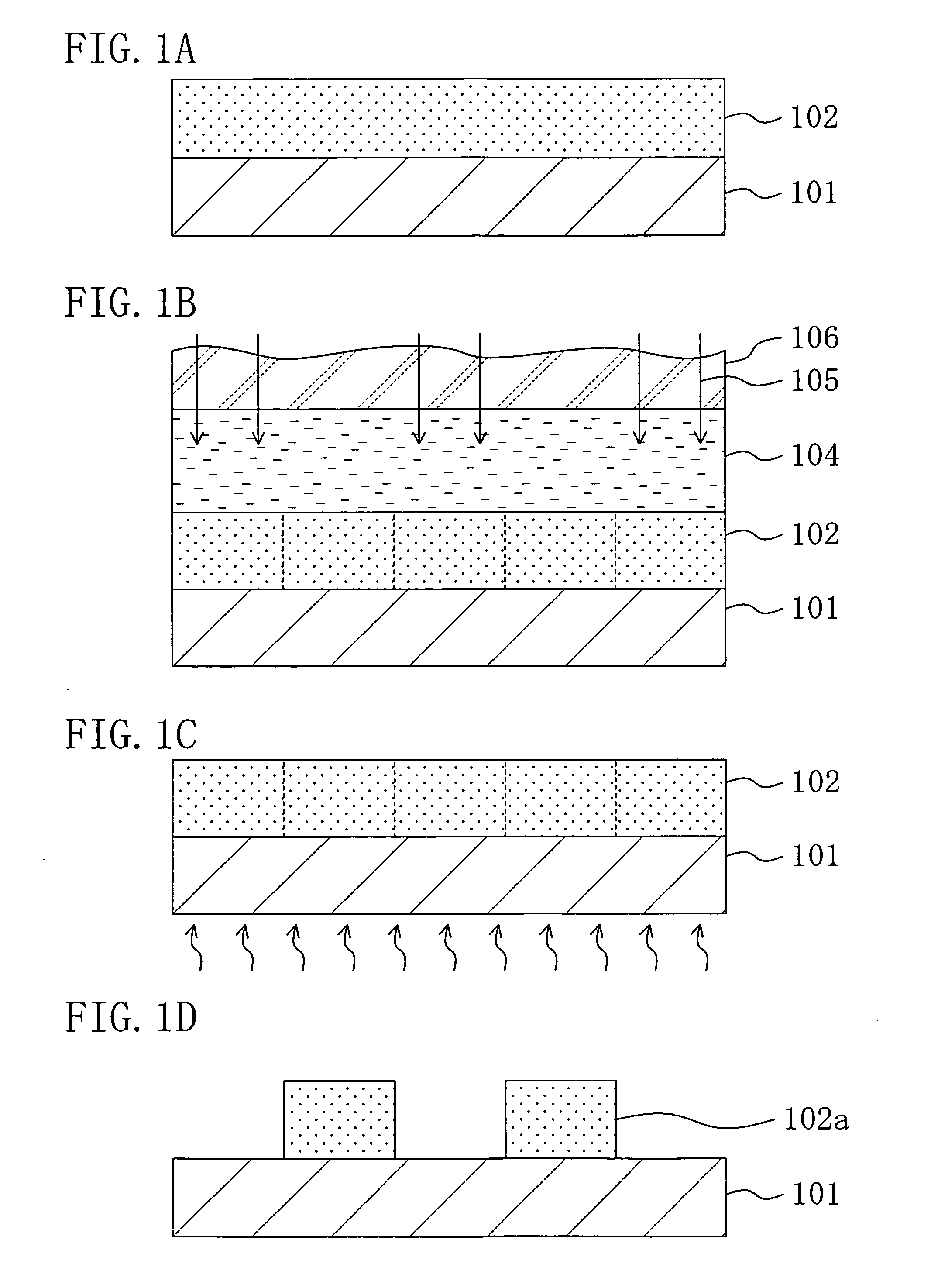
[0071] A pattern formation method according to Embodiment 1 of the invention will now be described with reference to FIGS. 1A through 1D.

[0072] First, a positive chemically amplified resist material having the following composition is prepared:

Base polymer: poly((norbornene-5-methylene hydroxymethyl2gcarboxylate) (50 mol %) - (maleic anhydride) (50 mol %))Acid generator: triphenylsulfonium trifluoromethane sulfonate0.04gQuencher: triethanolamine0.002gSolvent: propylene glycol monomethyl ether acetate20g

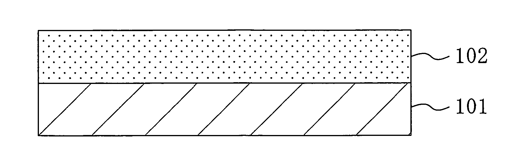
[0073] Next, as shown in FIG. 1A, the aforementioned chemically amplified resist material is applied on a substrate 101 so as to form a resist film 102 with a thickness of 0.35 μm.

[0074] Then, as shown in FIG. 1B, with an immersion liquid 104 of water provided between the resist film 102 and a projection lens 106 by, for example, a puddle method, pattern exposure is carried out by irradiating the resist film 102 through the liquid 104 with exposing light 105 of ArF excimer laser w...

embodiment 2

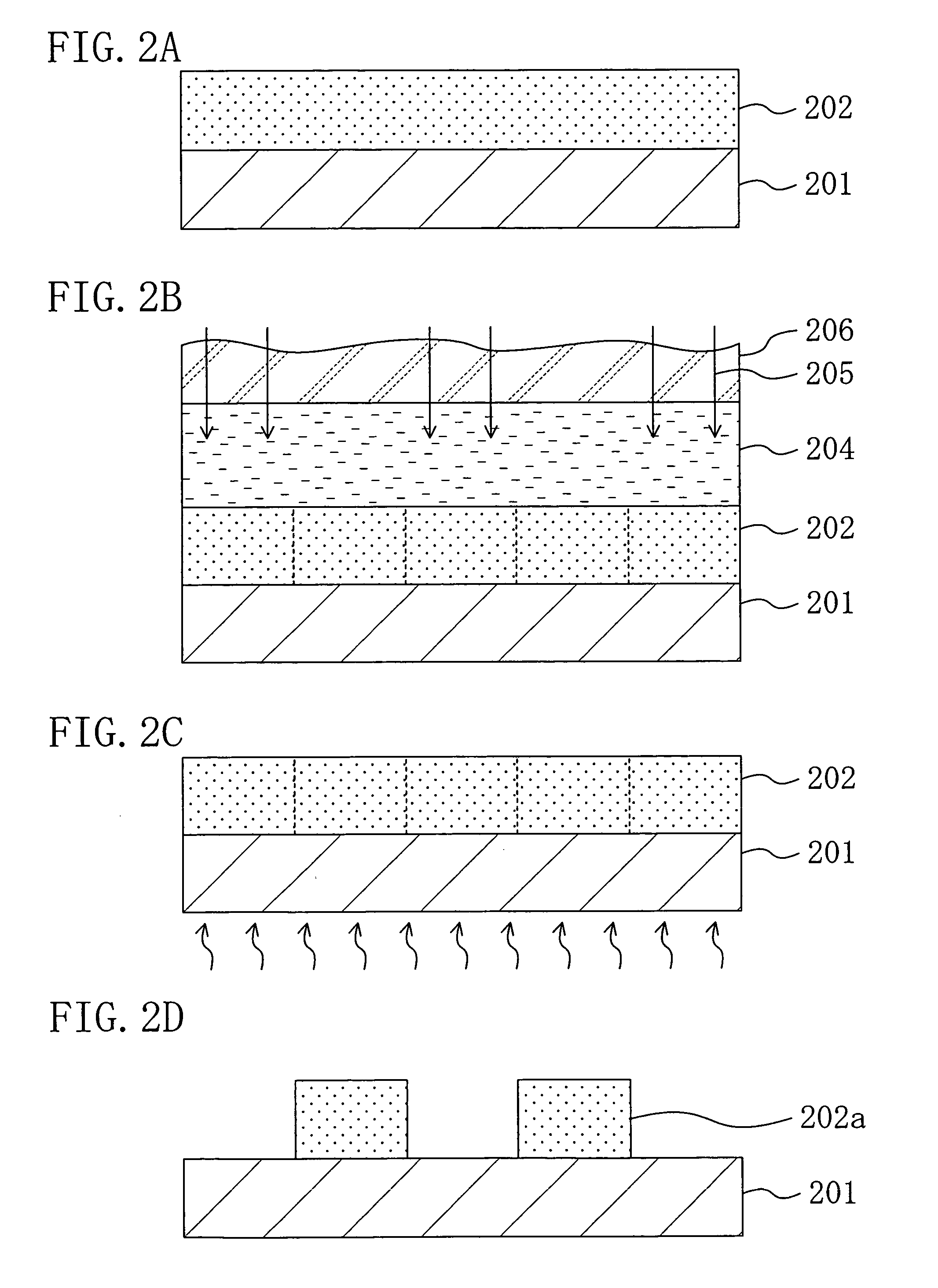
[0078] A pattern formation method according to Embodiment 2 of the invention will now be described with reference to FIGS. 2A through 2D.

[0079] First, a positive chemically amplified resist material having the following composition is prepared:

First base polymer: poly((norbornene-5-methylene2ghydroxyisopropyl carboxylate) (50 mol %) - (maleicanhydride) (50 mol %))Second base polymer: poly((norbornene-5-methylene0.08gmethoxymethyl carboxylate) (50 mol %) - (maleic anhydride)(50 mol %))Acid generator: triphenylsulfonium trifluoromethane sulfonate0.04gQuencher: triethanolamine0.002gSolvent: propylene glycol monomethyl ether acetate20g

[0080] Next, as shown in FIG. 2A, the aforementioned chemically amplified resist material is applied on a substrate 201 so as to form a resist film 202 with a thickness of 0.35 μm.

[0081] Then, as shown in FIG. 2B, with an immersion liquid 204 of water provided between the resist film 202 and a projection lens 206 by, for example, the puddle method, pat...

embodiment 3

[0087] A pattern formation method according to Embodiment 3 of the invention will now be described with reference to FIGS. 3A through 3D, 4A and 4B.

[0088] First, a positive chemically amplified resist material having the following composition is prepared:

Base polymer: poly((norbornene-5-methylene hydroxyethyl2gcarboxylate) (50 mol %) - (maleic anhydride) (50 mol %))Acid generator: triphenylsulfonium trifluoromethane sulfonate0.04gQuencher: triethanolamine0.002gSolvent: propylene glycol monomethyl ether acetate20g

[0089] Next, as shown in FIG. 3A, the aforementioned chemically amplified resist material is applied on a substrate 301 so as to form a resist film 302 with a thickness of 0.35 μm.

[0090] Then, as shown in FIG. 3B, by using a barrier film material having the following composition, a barrier film 303 having a thickness of 0.03 μm is formed on the resist film 302 by, for example, spin coating:

Base polymer: polyvinyl hexafluoroisopropyl alcohol 1 gSolvent: t-butyl alcohol2...


PUM


Abstract

In a pattern formation method, a resist film made of a chemically amplified resist material including a first polymer having hemiacetal or hemiketal is formed on a substrate. Then, with a liquid provided on the resist film, pattern exposure is performed by selectively irradiating the resist film with exposing light. After the pattern exposure, the resist film is developed so as to form a resist pattern made of the resist film.

Description

CROSS-REFERENCE TO RELATED APLICATIONS [0001] This application claims priority under 35 U.S.C. §119 on Patent Application No. 2005-174256 filed in Japan on Jun. 14, 2005, the entire contents of which are hereby incorporated by reference. BACKGROUND OF THE INVENTION [0002] The present invention relates to a chemically amplified resist material for use in immersion lithography and a pattern formation method using the same to be employed in fabrication process or the like for semiconductor devices. [0003] In accordance with the increased degree of integration of semiconductor integrated circuits and downsizing of semiconductor devices, there are increasing demands for further rapid development of lithography technique. Currently, pattern formation is carried out through photolithography using exposing light of a mercury lamp, KrF excimer laser, ArF excimer laser or the like, and use of F2 laser lasing at a shorter wavelength of 157 nm is being examined. However, since there remain a la...

Claims


Application Information

Patent Timeline
IPC IPC(8): G03C1/00
CPCC08L59/00C08L2205/02G03F7/0392Y10S430/106G03F7/2041C08L2666/16
Inventor ENDO, MASAYUKISASAGO, MASARU
Owner RPX CORP
Why Eureka
Try Eureka