

Optical measurement method and device
a measurement method and optical technology, applied in the field of optical characteristics measurement, can solve the problems of large loss of light quantity, difficult to achieve the space resolution of finer than one micron, and serious affecting device characteristics, etc., to achieve the effect of decreasing the scattering of exciting ligh
- Summary
- Abstract
- Description
- Claims
- Application Information
AI Technical Summary
Benefits of technology
Problems solved by technology
Method used
Image

Examples
example 1
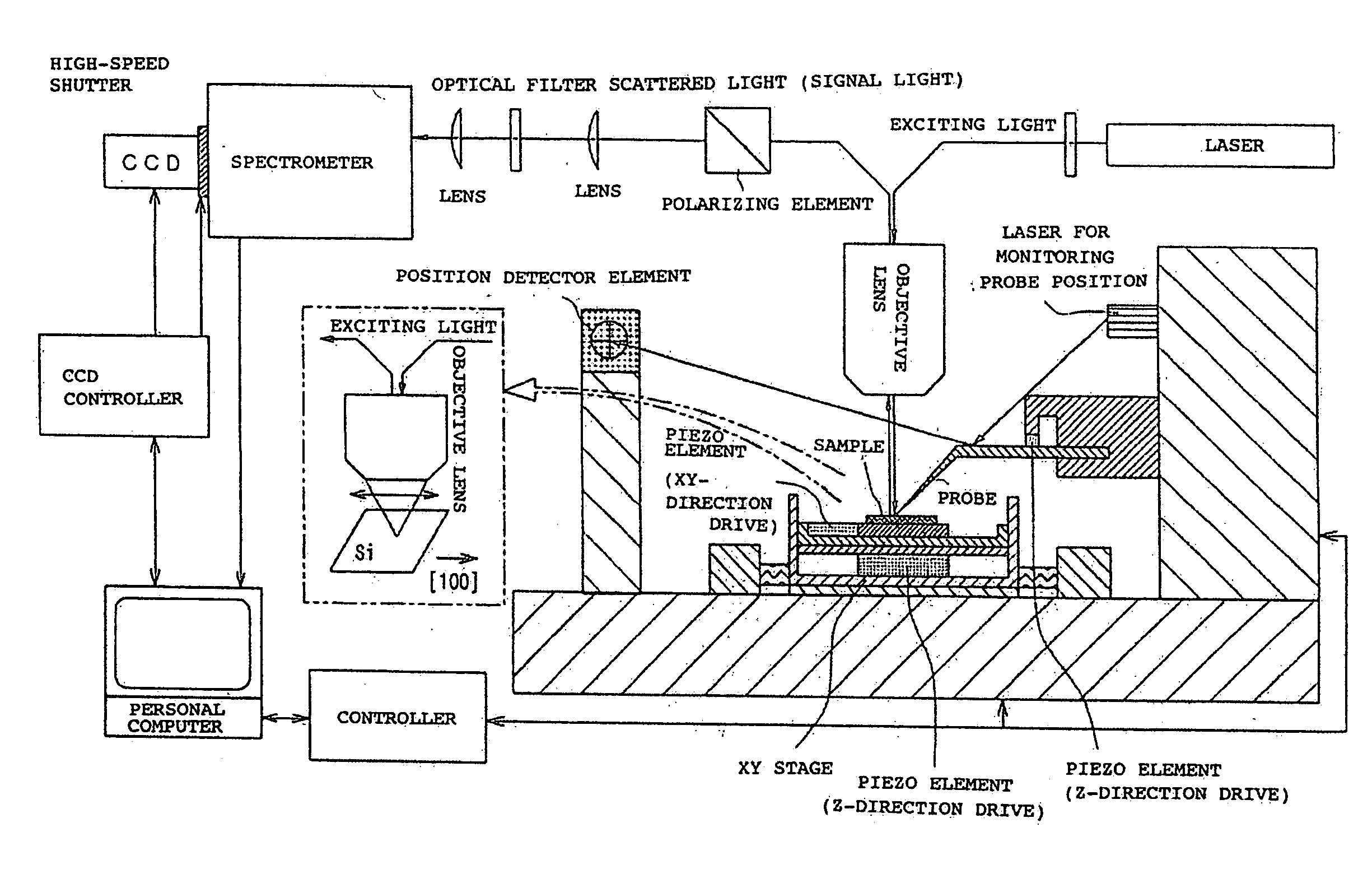
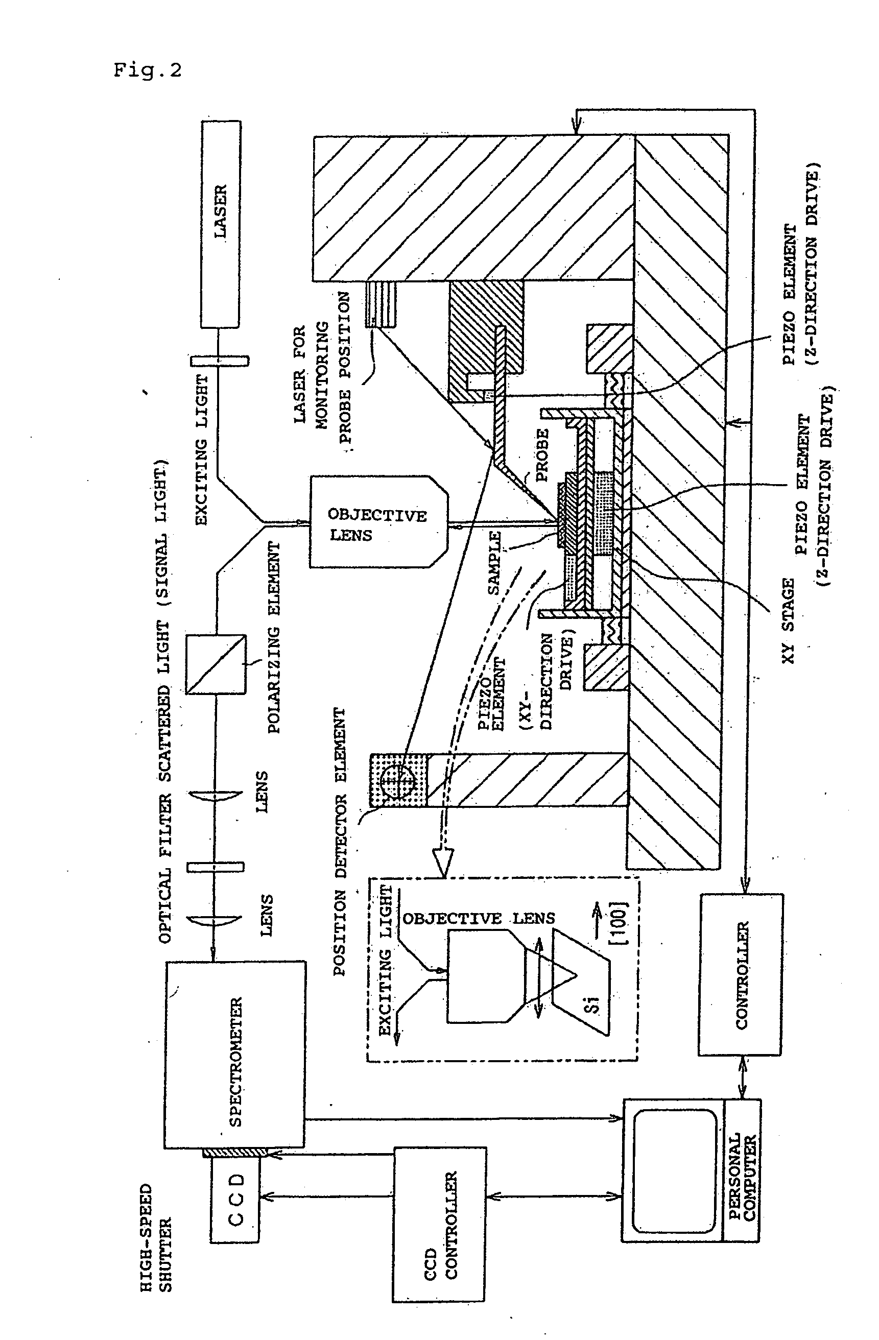
[0071]FIG. 2 is a diagram schematically illustrating the arrangement for measurement. The AFM probe coated with silver is mounted on a piezo element and can be vibrated up and down by signals from a controller. Further, a piezo element is mounted on a stage on which a sample holder is mounted, and can be driven up and down and right and left by signals from the controller. The exciting laser beam is focused on the surface of a sample by an objective lens, and the AFM probe coated with silver is brought close to the focusing portion. The operation of the AFM probe is controlled by the light from a laser diode and by a detector. As shown, the laser beam for excitation is caused to so fall as to be polarized in [100]. Of the scattered light collected by the objective lens, the scattered light polarized in [100] only is guided to a spectrometer and is separated.
[0072] More concretely, the laser beam of 514.5 nm or 632.8 nm is caused to fall on a (001) substrate of Si perpendicularly th...
example 2
[0074] The following measurement is conducted to prove a high spatial resolution of the measurement method of this Example. Referring to FIG. 4(a), the sample is a 5 μm wide island of a strained SOI (silicon-on-insulator) thin film formed by epitaxially growing Si in a thickness of 14 nm on the (001) surface of SiGe (Ge composition of 28%) of a thickness of 40 nm. Here, a laser beam of 514.5 nm is caused to fall in a manner that the polarization direction thereof is in parallel with [100]. The scattered light of which the polarization direction is in parallel with [100] only is detected by using a polarizer. FIG. 4(a) illustrates changes in the Raman spectra near the edge of the SOI island, and (b) illustrates changes in the Raman shift.
[0075] Strained Si and Si have different lattice constants, therefore the peak position of the Raman spectra shifts from ordinary 520 cm−1 to ˜515 cm−1. The probe is scanning from the edge of the island to its interior region while monitoring the pe...
example 3
[0076] The measurement is taken in the same manner as in Example 2 but using a tip having diameter of 50 nm. The spatial resolution is about 50 nm.
PUM
 Abstract
Description
Claims
Application Information