Copper alloy for electronic machinery and tools and method of producing the same

a technology of electronic machinery and tools and copper alloy, which is applied in the direction of metal rolling stands, solid-state devices, metal-working apparatus, etc., can solve the problems of bringing about a rise in soldering temperatures at the time, and lowering the bonding strength of wire bonding, so as to achieve excellent plating with metals, reduce the adhesiveness of oxidation film, and not precipitate anomalous metal plating. , the

Inactive Publication Date: 2007-01-18
FURUKAWA ELECTRIC CO LTD
View PDF2 Cites 23 Cited by
  • Summary
  • Abstract
  • Description
  • Claims
  • Application Information

AI Technical Summary

Benefits of technology

[0009] In accordance with the present invention, a copper alloy having an excellent platability with metals and causing neither anomalous precipitation of plating metals nor lowering of adhesiveness of oxidation film can be provided for use in electronic machinery and tools.

Problems solved by technology

From the viewpoint of environmental issues, the solder used in mounting those components on boards has been required to be free of lead, and then many lead-free solders bring about a rise in soldering temperatures at the time of mounting on boards.
As pitches are narrowed, problems may be caused in the producing method of lead frames.
Specifically, there may be cases in which the Ag plating given in the producing method of lead frames causes anomalous precipitation and growth to a projecting form, thereby lowering the bonding strength of wire bonding, and shorts may occur between adjacent leads.
In these areas also, anomalous precipitation, for example, porous precipitation, of the Cu plating causes formation of oxide film inferior in adhesiveness on the lead frame surface, to result in lowering of adhesion between a mold resin and lead frames.
Thus, the problem occurs that, when soldering onto boards is carried out, packages become cracked in a reflowing furnace.
However, these methods, though effective on copper alloys having specific alloy compositions, cannot be applied to other copper alloys.

Method used


Image

  • Copper alloy for electronic machinery and tools and method of producing the same
  • Copper alloy for electronic machinery and tools and method of producing the same

Examples


example 1

[0056] Copper alloys having chemical compositions shown in Table 1 were made into 0.15-mm thick copper alloy sheets by undergoing casting, rolling, buff polishing and annealing in succession. These copper alloy sheets were each given degreasing treatment and pickling treatment, and then subjected to treatment for removal of their respective work affected layers by chemical dissolution. Each of the thus treated materials was coated with Ag plating, and Ag platability was evaluated.

TABLE 1AlloyAlloy composition (mass %)No.CrSnZnNiSiMgFePAgMnCuA0.30.250.2BalanceB3.00.650.15BalanceC0.152.30.03BalanceD0.15BalanceE0.52.50.60.030.1Balance

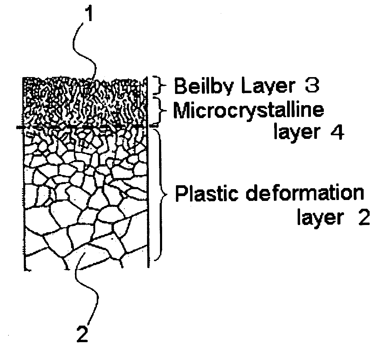
[0057] The degreasing treatment was performed by cathodic electrolysis for 30 seconds in a degreasing solution, which contained 60 g / l of Cleaner 160S (trade name, produced by Meltex Inc.) and was kept at a temperature of 60° C., under a current density of 2.5 A / d m2. And the pickling treatment was performed at room temperature by immersion for 30 second...

example 2

[0062] Ag plating was performed in the same manner as in Example 1, except that electrolytic dissolution was used as the method of removing the work affected layer of each copper alloy, and the Ag platability was evaluated using the same criteria as in Example 1.

[0063] The removal of the work affected layer of each copper alloy was performed by anodic electrolysis in an aqueous solution containing 700 g / l of phosphoric acid at room temperature under a current density of 10 A / dm2. Herein, five specimens of each copper alloy were prepared for examples of the present invention so that their individual work affected layers after the removal treatment had thicknesses of 0, 0.02, 0.05, 0.1 and 0.2 μm, respectively; while one specimen of each copper alloy was prepared for a comparative example so that its work affected layer after the removal treatment had the thickness of 0.3 μm.

[0064] Evaluation results in Example 2 are shown in Table 3.

TABLE 3AlloyThickness of workEvaluation of AgRe...

example 3

[0065] Ag plating was performed in the same manner as in Example 1, except that heat treatment was used as the method of removing the work affected layer of each copper alloy, and the Ag platability was evaluated using the same criteria as in Example 1.

[0066] The removal of the work affected layer of each copper alloy was performed by heat treatment of 2 hours in a heating furnace with a reducing atmosphere of hydrogen. Herein, five specimens of each copper alloy were prepared for examples of the present invention so that their individual work affected layers after the removal treatment had thicknesses of 0, 0.02, 0.05, 0.1 and 0.2 μm, respectively; while one specimen of each copper alloy was prepared for a comparative example so that its work affected layer after the removal treatment had the thickness of 0.3 μm.

[0067] Additionally, for reducing the thickness of the work affected layer of each copper alloy to 0, 0.02, 0.05, 0.1, 0.2 and 0.3 μm from the original value of 0.4 μm, t...


PUM

PropertyMeasurementUnit
thicknessaaaaaaaaaa
grain sizeaaaaaaaaaa
thicknessaaaaaaaaaa

Abstract

A copper alloy for electronic machinery and tools, having a surface layer of a work affected layer whose thickness is 0.2 μm or below; and a method of producing the same.

Description

TECHNICAL FIELD [0001] The present invention relates to a copper alloy improved in platability with metals. BACKGROUND ART [0002] Copper alloys used in electronic machinery and tools are given various kinds of metal plating, seeking to impart more functionality thereto. In their use for lead frames, for example, they are given Ag plating for wire bonding, Cu plating as a foundation for the said Ag plating, and solder plating for mounting on boards. [0003] Recent years have also seen the use of plated lead frames prepared by giving metal plating throughout the surface of lead frames after forming lead by etching or presswork. The metal plating given therein includes Pd plating, and Ni plating as a foundation thereof. [0004] In recent years, further increases in packing density and further reductions in size and profile have been required of electronic components used in electronic machinery and tools. In response to these requirements, efforts have been moving ahead to increase the n...

Claims


Application Information

Patent Timeline
Patent Type & Authority Applications(United States)
IPC IPC(8): B32B15/00C25D5/10
CPCC25D5/34Y10T428/1291H01L23/49579H01L23/49582H01L2924/00014H01L2924/01019H01L21/4842Y10T428/12903Y10T29/49991Y10T428/12694H01L2924/0002Y10T428/12472Y10T428/12507Y10T428/12514Y10T428/12792Y10T29/49002Y10T428/12771H01L2224/45099H01L2924/00C22C9/02C22C9/04C22F1/02C22F1/08
Inventor UNO, TAKEOSUGAHARA, CHIKAHITOMIHARA, KUNITERU
Owner FURUKAWA ELECTRIC CO LTD
Why Eureka
Try Eureka